The Era of Tera: Intel Reveals more about 80-core CPU
by Anand Lal Shimpi on February 11, 2007 5:44 PM EST- Posted in
- CPUs
The Chip
As its name implied, the Teraflops Research Chip is a research vehicle and not a product. Intel has no intentions of ever selling the chip, but technology used within the CPU will definitely see the light of day in future Intel chip designs.
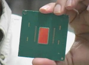
The Teraflops chip is built on Intel's 65nm process and features a modest, by today's standards, 100M transistors on a 275mm^2 die. As a reference point, Intel's Core 2 Duo, also built on a 65nm process, features 291M transistors on a 143mm^2 die. The reason the Teraflops chip is large given its relatively low transistor count is that there's very little memory on the chip itself, whereas around half of Intel's Core 2 is made up of L2 cache. Other than being predominantly logic circuits, the Teraflops chip also has a lot of I/O circuitry on it that can't be miniaturized as well as most other circuits resulting in a larger overall chip size. The chip features 8 metal layers with copper interconnects.
The Teraflops chip is built on a single die composed of 80 independent processor cores, or tiles as Intel is calling them. The tiles are arranged in a rectangle 8 tiles across and 10 tiles down; each tile has a surface area of 3mm^2.
The chip uses a LGA package like Intel's Core 2 and Pentium 4 processors, but features 1248 pins. Of the 1248 pins on the package, 343 of them are used for signaling while the rest are predominantly power and ground.
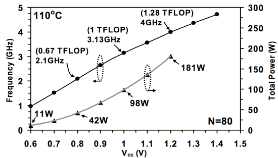
The chip can operate at a number of speeds depending on its operating voltage, but the minimum clock speed necessary to maintain its teraflop name is 3.13GHz at 1V. At that speed and voltage, the peak performance of the chip with all 80 cores active is 1 teraflop while drawing 98W of power. At 4GHz, the chip can deliver a peak performance of 1.28 TFLOP, pulling 181W at 1.2V. On the low end of the spectrum, the chip can run at 1GHz, consuming 11W and executing a maximum of 310 billion floating point operations per second.


25 Comments
View All Comments
F1N3ST - Monday, February 19, 2007 - link
800 cores for 10 TFlops I say.jiulemoigt - Wednesday, February 14, 2007 - link
maybe 80 un-synced in-order chips is pointless but that stack as a mem controller80 socketed un-synced in-order chips is pointless, since most of the functionally comes from branch logic and out-of-order operations, and not syncing them together means that you could not pass data through them only to them, and even then, issues with passing data would be a mess.
Yet that stack sitting underneath a modern cpu, especially if it could be used as a modern memory stack, with cache speed data access to four cores, that would speed many corp customers could use. Though the memory controller on the chip in the center to control the data flow treat the system memory as virtual extension of it, just like modern hard drives are virtual extensions of system memory, now we are a talking about access data as fast as we can use it. Though the branch logic is going to have to get even better.
najames - Monday, February 12, 2007 - link
Remember the Itanimum and the BILLIONS of dollars Intel spent on the thing? Remember how they thought every company would buy them by the truckload? Remember how expensive they were?Intel did deliver on the Core 2, but I am still leary of anything they hype up.
Brian23 - Monday, February 12, 2007 - link
I know that this chip won't run x86 code, but how does a Core 2 Duo 6600 compare to this as far as teraflops go?AnnihilatorX - Monday, February 12, 2007 - link
I believe that due to physical structures of the silicon lattice silicon is just not a good material candidate for a silicon-on-chip design. Exact same reason why blue laser diodes are made of Gallium arsenide rather than silicon.It's time to move on the much faster and better material than silicon.
fitten - Monday, February 12, 2007 - link
Yes, but silicon has the advantage of beinga) very cheap, comparatively
b) plentiful
benx - Monday, February 12, 2007 - link
I think it is time to stop building computers around the van neumann cycle idea. There wil always be the FSB preformance hit. To counter the problem cpu builders just add more L1/L2/L3 and now maybe L4?time to make the intel cycle with out fsb =)
fikimiki - Monday, February 12, 2007 - link
80 cores sounds great for webserver, java or paralell-processing but how does it stand against to the price and performance of 4 x QuadCore stacked on a single board?Intel is trying to achieve the same thing as Transmeta or just show the marketing muscle once again. I'm sure that Teraflop is going to loose with specialized variety of chips like nVidia, ATI, Cell or Opteron together. You put 3-4 of those and that's it.
We hear that R580 (ATI) can run some calculations 20x faster than ordinary x86, the same with Cell so what the hell is teraflop chip? Especially with integer only calculations?
JarredWalton - Monday, February 12, 2007 - link
I think you're missing the point of this article and the processor. Intel has no intention of ever releasing this particular Teraflop chip into the mainstream market. This is an R&D project, nothing more nothing less. All you have to do is look at the transistor counts to realize that performance isn't going to be competitive right now. Intel chose 80 cores simply because that was what fit within their die size constraints. If they could've fit 100 cores, they would have done that instead.In the future, Intel is going to take some of what they've learned with this research project and apply it to other processors that they actually intend to mass produce and sell. That probably won't happen for several more years at least, and when they get around to releasing those chips you can be sure that they won't have 80 cores and that the course of that they do have won't be anything like the simple processing units on this proof of concept.
How long before anything like this ever becomes practical on desktop computers? How long before it becomes necessary? Those are both interesting questions, and software are obviously has a long way to go first. I have no doubt that someday people are going to have computers with dozens of processor cores sitting on their desktops and in their laptops. Whether that's going to be in 10 years or 100 years... time will tell. I just hope I'm around long enough to see it! :-)
Andrwken - Monday, February 12, 2007 - link
Basically they are just using it as a proving ground to show what can be done when more bandwidth is needed than traditional fsb and hypertransport can deliver. It would definitely be worthwhile in a configuration with say 20 cores and using 8 for cpu, 8 for video, and 2 for physix (one example). But my question is, doesn't this kind of go along with the supposed programmable generic cores that intel wants to use in their new discreet graphics cards? If so, it could be supposed that the code for this kind of monster is already being worked out and one multicore chip can be programmed to use each core as necessary, finally eliminating all the discreet cards and levying the power of one large multicore chip as needed? (sony came close with POS3 but still needed a discreet graphics chip at this point) They get the programming down with the discreet graphics cards and then use that for single chip integration down the road. That's just how I am reading into it and I may be way off base, but this tech maybe much closer to viable than we are giving it credit for. Especially in a cheap laptop or small formfactor application.