Original Link: https://www.anandtech.com/show/355
We all owe something to AMD, regardless of what processor you use in your system now, chances are that your buying decision was somehow influenced by AMD. Intel advocates enjoyed the benefits of more competitive pricing and accelerated processor release schedules that put faster processors in the hands of the masses at a cheaper price. AMD supporters obviously enjoyed the benefits of an alternative to Intel and a chance to root for the underdog, something the market has a general tendency of doing. Even for AnandTech, AMD provided us with a start back in April 1997 with the release of the K6 microprocessor, it was that processor release that originally sparked the idea to start AnandTech a little over two years ago.
For those of you that weren’t much into the desktop x86 processor market in 1997 let’s set the scene. Intel’s greatest competition in the desktop processor market was Cyrix with their 6x86-PR200+, a processor that did nothing but confuse potential buyers by its 150MHz operating frequency. AMD’s threat to the market share was insignificant after receiving a huge blow to their reputation courtesy of the incredible delay in releasing the K5 processor. Intel’s Pentium was nearing the end of its life span at 200MHz and the Pentium Pro 200 was keeping high end users happy by providing excellent performance and support for heavy-duty multiprocessor servers. The hardware enthusiast looking for an increase in power could always pursue a dual Pentium system that was considerably cheaper than a single processor Pentium Pro system.
Wednesday morning, April 2nd, 1997 marked the date of the introduction of the AMD K6 processor. The rumors that surrounded the release included the leaked information that the K6-200 would be able to compete with the Pentium Pro 200 and undercut Intel’s costs by a margin of around 25%. Others claimed that the K6 would be the return of competitive non-Intel CPUs, an increasing rarity since the release of the 486. The nondisclosure agreements expired, the information embargoes were lifted, and the results published. The K6 ended up being more of a competitor to Intel’s latest Pentium MMX than the Pentium Pro, and for games, the K6 was considerably slower than Intel’s offering at similar clock speeds. The K6’s FPU was dubbed weak, and the processor entitled a low cost solution. A problem with supplying the chips to end users [at a reasonable cost] was a major issue that the ill-fated company later became known for. Who would’ve expected that AMD would be doomed to the flaws of the K6 for the next two years and that the return of the Intel competitor would put AMD chips mainly in low cost systems and tarnish the name as an underdog, and nothing more.
Tried and Failed
With every processor release following the K6, the hopes remained high, but the results were generally disappointing. The next "big break" for AMD came with the rumors that a 266MHz K6 would make it out in time for a November ’97 launch which would once again pit AMD against Intel in a battle of clock speeds. With Intel pushing the Pentium II to speeds of 300MHz and receiving decent yields using the same 0.35-micron process they had been using with the Pentium MMX AMD needed to compete on a clock for clock basis. The only way a K6 faster than 233MHz could be produced would be on a 0.25-micron fabrication process. Rumors began to surface about extremely poor yields on 0.25-micron parts from AMD and the release of the 266MHz K6 was pushed back to early 1998, around February the parts became available but Intel had already moved to 0.25-micron and was pushing 333MHz.
The next opportunity for AMD came with addressing their weakness, their FPU. AMD was in a lose-lose situation, they weren’t able to produce enough processors to compete with Intel solely on clock speed, and at the clock speeds they were currently at, they weren’t able to produce high enough performing parts to make a significant difference in the market share. Granted they were making progress, but the outlook didn’t seem good. Rumors (you’ve gotta love those) began to surface about a mysterious K6-3D processor, supposedly a 300MHz K6 with an improved FPU, possibly one that could match or even exceed Intel’s current offerings at a lower cost. AMD’s policy became to undercut Intel’s pricing whenever possible, however sometimes it just wasn't possible. AMD was involved in a price war, one that they were trying very adamantly to win, but as we've seen in the past, often when a company is involved in a price war, they stop worrying about competing on other levels, including performance.
A New Hope
May 1998, Atlanta, Georgia, the E3 Expo was the introduction arena for AMD's "sure fire win" against Intel, the K6-2, formerly known as the K6-3D. The elegant fix to AMD's FPU problem was not throwing more raw performance at the applications that made the original K6 choke rather giving it the ability to more efficiently use the power it did have. The technology? 3DNow!
The 21 instructions that made up 3DNow! were not revolutionary, but they were a step in the right direction. For once AMD was the market leader in a step that the rest of the industry would follow through with, the step was towards a technology known as SIMD. Intel actually made the first move towards Single Instruction Multiple Data execution with their 57 MMX instructions that did so very little with the Pentium MMX and Pentium II. The whole idea behind SIMD execution is that if you're performing one operation on multiple types of data, why not perform that one operation on all the data simultaneously instead of waiting for the operation to be completed on one set of data before repeating the process. Therefore we get the basic definition of SIMD, or Single Instruction Multiple Data (in this case SIMD-FP as it applies to FPU instructions, whereas MMX offered SIMD-Int for Integer instructions) a hardware algorithm that allows a single command (or instruction) to be applied to multiple sets of data simultaneously.
The problem with Intel's MMX instructions was that the only type of SIMD being used was SIMD-Int, for integer based calculations, an area that honestly wouldn't benefit considerably from SIMD execution capabilities. Using Intel's branding, the term MMX became a household name while the majority of hardware enthusiasts were complaining about the uselessness of the technology. What AMD did was apply the SIMD execution algorithm to Floating-Point instructions, thus resulting in SIMD-FP, and also resulting in a significant increase in FP performance. As it seemed, AMD had finally won and Intel's "tyrannical" reign was over, the K6-2, with 3DNow! support was able to beat the Intel Pentium II in games that took advantage of the 21 new instructions. Then came the Celeron…
Crushing Dreams
Intel's low cost competitor to AMD's platform, the Celeron, was what forced AMD into yet another price war. AMD would drop prices, then Intel would drop them even lower on the Celeron line. Intel had the ability to drop the prices of a line that was relatively inexpensive to manufacturer, and could compete on a clock for clock basis with AMD's latest and greatest. AMD was struggling once again, this time motherboard manufacturers didn't seem to support AMD's Super7 platform as well as the K6-2 demanded. Graphics card incompatibility problems and poorly manufactured motherboards plagued the platform.
In November of 1998, AnandTech was able to take a look at AMD's next attempt at winning back the performance market, the K6-3. Later renamed to the K6-III (it's amazing what three I's can do), the processor took the Celeron route and integrated a full 256KB of L2 cache onto the die of the processor therefore operating at the processor's clock speed and giving the fastest Pentium IIs a run for their money. By this time, 3DNow! was being implemented in more and more games, however the K6-III still lagged behind in terms of non-optimized FP code not to mention the continuing motherboard issues and chipset incompatibilities. Not more than three days after we previewed the K6-III, the first person to ask us the million-dollar question appeared in our mailboxes, "When will you be previewing the K7?"
The First Encounter
| We first took a look at the upcoming AMD K7 slightly before this year's E3 Expo, as fate would have it, around the same time as the release of the K6, just two years ago. The performance of the K7, then clocked at 500MHz, was on par with a Pentium III 500. The system bus operated at a unique 125MHz, and AGP support was very limited. Needless to say, we were not impressed. |

The second encounter resulted in more positive results, in all but one test, the K7 550 managed to beat the Pentium III 500. The one test that resulted in a considerably lower score on the part of the K7 was Ziff Davis' FPU Mark, luckily the problem turned out to be related to a hardware bug with the CPU, one that was later fixed. The important thing to keep in mind at that point was that AMD had actually produced a chip, albeit still in beta stages, that could compete with a Pentium III, clock for clock, across the board, in games and business applications. The potential was there, but could AMD do it?
AMD promised a June release of the K7, and in June AMD approached us about reviewing the K7 now clocked at 600MHz and ready for action. Without refusing the NDAs were signed, and the system was in our hands. The results? Well, you're about to find out.
Take your K6 and shove it
AMD has had a reputation for some of the worst possible things a CPU manufacturer can be known for. They have been known for being slow to market, poor performers, incompatible, and by many, the name to stay away from. At the same time, there are users that swear by AMD, there are users that wouldn't dream of touching an Intel CPU and they're more than happy with their K6-X systems. What should both types of users assume of AMD's latest? Nothing at all, what was once known as the K7, is the first in a revolution for AMD as a CPU manufacturer. So take whatever you know and remember about the K6 line of processors and forget it, AMD built the K7 from scratch, and they have a new name to signify it, the name is Athlon.
Whereas the K6-2 and K6-III were essentially building blocks based on the original K6 foundation, the Athlon is a completely new design. It is the first 7th generation x86 processor to come to market, a move that the industry expected to be made first by Intel, and it is no doubt that AMD's sudden surfacing has startled more than a few people.
The Basics
The Athlon is the first non-Intel x86 CPU to move away from the conventional socketed design in favor of a slot interface connector. Intel made the move to the 242-pin Slot-1 connector with the Pentium II and received quite a bit of heat for doing it, with accusations of them attempting to kill all competition with this proprietary connector. In all fairness, all you Intel supporters now have the right to say the same thing about AMD :)
But regardless of what company you support, the truth of the matter is that a slot design is easier on the user from the point of installation. Ask any system builder and he/she will tell you that sticking in a Slot-1 processor without the fear of bending pins is much easier than working with a socketed CPU.
The Athlon interfaces using a 242-pin slot connector known as Slot-A. Before you get excited about AMD's decision to use a 242-pin slot connector, the only reason AMD chose to implement a physically similar slot connector to Slot-1 was to make it easier on the motherboard manufacturers. Instead of having to worry about new PCB designs and connectors, motherboard manufacturers can simply reuse most of their basic designs, flip their Slot-1 connectors around, and have the start of a Slot-A motherboard.
Intel's 242-pin Slot-1 connector
![]()
AMD's 242-pin Slot-A connector
![]()
The 242-pin Slot-A connector is essentially a Slot-1 connector, flipped backwards. The reasoning behind this is simple, it looks like a Slot-1 connector, but neither you nor AMD wants a user trying to stick a Slot-1 processor in a Slot-A motherboard, why? Because although Slot-1 and Slot-A are physically similar, the interfaces provide a connection to two completely different architectures, meaning that you can't just plug one processor into the other slot. The differing architectures will be discussed shortly, but first let's talk about the CPU.
The Athlon is manufactured on a 0.25-micron fabrication process, the standard for both Intel and AMD currently. At the same time, there are plans to move the Athlon to 0.18-micron production definitely in the year 2000 if not earlier. Intel is preparing the same move with their Coppermine processor later this year, however AMD isn't blessed with the same fab plants Intel has worked hard for so the Athlon will currently ship on a 0.25-micron die.
| The 184 mm2 die is composed of 22 million transistors, the highest transistor count for an x86 processor's core to date. A large portion of the 22 million transistors is dedicated to the 128KB of L1 cache the Athlon boasts, an increase over the 64KB L1 on the K6-3 and the 32KB L1 on the Pentium III. The real world benefits of a large L1 cache are mainly seen in business application performance, especially with applications that fit directly into the L1 cache of the processor. Operating at the clock speed of the processor, the 128KB of L1 gives the Athlon a major advantage in terms of business application performance, an area that has always been a strongpoint for AMD. |

The 128KB of L1 operating at clock speed is accompanied by a Pentium II/III-esque L2 cache operating at a fraction of the clock speed located on the processor card. The Athlon architecture allows from 512KB up to 16MB of L2 cache to be included on the processor's card, however the first shipping Athlons will feature 512KB. Like the Pentium II/III, the Athlon's 512KB of L2 cache operates at 1/2 the core clock speed, but the flexible architecture allows for the L2 cache to operate at other fractions such as 1/3 clock speed or even at clock speed like Intel's Xeon processor. The reason for such a wide range of supported options is so that AMD can branch out and produce a number of different Athlons, such as a low cost Athlon (like Intel's Celeron), and a high end Athlon with a larger, faster cache. AMD's roadmap calls for the Athlon branding to split into multiple types of Athlon processors. This mimics how the original Pentium II has grown into the Intel Celeron for the low end/entry level, the Intel Pentium III for the mainstream, and the Intel Pentium III Xeon for the high end users.
| The L2 cache on the Athlon, like the Pentium III, is present via two 2Mbit chips with no external Tag-RAM. The processor card itself is identical to the original SECC specification Intel used with the Pentium II, unfortunately the mounting holes on the card itself are different from those on the older Pentium IIs and the newer Pentium IIIs/Celerons. The cooling plate attached to the Athlon makes contact with both L2 cache chips and the core itself. |

The Athlon will be initially released in 500, 550, and 600MHz parts with L2 caches running at 250, 275, and 300MHz respectively. In early September, AMD will officially launch the 650MHz Athlon (325MHz L2), which is ahead of their original schedule. Not only is AMD attempting to go head to head with Intel in a clock speed battle, they are looking to beat them in performance at each clock frequency. The 600MHz Athlon processors AMD shipped to reviewers featured 3.3ns NEC made L2 cache, which mathematically is able to handle the 300MHz operating frequency the 600 demands. The current specification of the 500 - 650MHz parts call for a core voltage setting of 1.6v, which is 0.4v less than the Pentium III's voltage 2.0v requirement.
| In terms of pricing, AMD expects the 500 to sell for $249, the 550 for $449, the 600 for $615 and the 650 for $849 in quantities of 1000. So for those of you expecting AMD to be able to undercut Intel's pricing with the Athlon, think again, the Athlon will be competitively priced, but definitely not a cheap processor. |

EV6 & the Athlon's Busses
We discussed earlier that although the Athlon's Slot-A connector was physically similar to the Pentium III's Slot-1 connector, the processors are not interchangeable. The reason behind this is that the two processors operate on different system, or front side, busses. The front side bus (FSB) is the connection between the CPU and the chipset, and the bus Intel has been using with the Pentium II/III, Xeon and Celeron processors is known as the GTL+ bus. GTL+ operates at 100MHz and thus provides 800MB/s of bandwidth (64-bits x 100MHz = 6400 Mb/s / 8 = 800MB/s). Intel is pushing to increase the FSB specification of GTL+ to 133MHz later this year with the Camino chipset, which would increase the available bandwidth between the CPU and chipset to a little over 1GB/s of bandwidth. For a single processor system, saturating the 800MB/s of bandwidth doesn't occur too often when you consider that a large percentage of users still only use their computers for word processing and web surfing.
| Saturation of the 100MHz GTL+ bus
happens most frequently in high-end workstations and servers, and is especially easy to
point out in multiprocessor systems. The GTL+ bus is a shared bus, meaning that regardless
of how many processors you have present in your system, they must all share the same
800MB/s of bandwidth. This is part of the reason that adding more than two processors to
an Intel Xeon server begins to give you diminishing returns, and it is also part of the
reason that many companies pursue multiple dual processor servers versus a handful of quad
processor servers. Intel's GTL+ Shared Bus (right) |
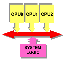 |
| Take a single Intel Pentium III Xeon for example, there is 800MB/s of bandwidth available for use with the current GTL+ bus. Adding a second processor into the system cuts the bandwidth available per processor down to 400MB/s. Adding two more processors leaves each CPU with 200MB/s of available bandwidth between the CPUs and the chipset. See the problem? | |
AMD chose a different approach, rather than attempt to license GTL+ for use with the Athlon, AMD went around Intel and straight to Digital, the manufacturers of the powerful Alpha processor. Using Digital's EV6 bus protocol, AMD was able to give the Athlon a much greater potential for growth. On the transfer side of things, EV6 allows for 64-byte burst data transfers versus the 32-byte burst data transfers supported by GTL+. Translation? The EV6 is inherently capable of sending more data at a time through the bus than GTL+. The EV6 bus also adds the security of 8-bit ECC to all data transfers, a feature already implemented by Intel in the GTL+ bus but absent from all Super7 platforms.
The big difference between EV6 and GTL+ in the minds of those that first hear about it seems to be the operating frequency of EV6. The beauty of EV6 is that it takes advantage of the same technology that is behind the accelerated graphics port, or AGP in that it allows data to be transferred on both the rising and falling edges of the clock. This allows the memory bus to operate at 100MHz while delivering 200MHz (1.6GB/s of bandwidth) between the chipset and CPU because it delivers twice as much information, by transferring data on both the rising and falling edges of the clock. This allows for 1.6GB/s of bandwidth available for a single Athlon processor, but that's not where the beauty of EV6 ends.
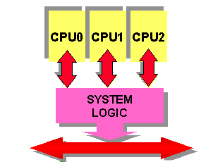
| EV6 offers a point-to-point
connection for multiprocessor systems, meaning that each processor added to the equation
gets its own 200MHz or 1.6GB/s of bandwidth to the chipset. Theoretically, this takes a
huge chunk of the diminishing returns away from adding multiple processors to a system
based on the EV6 bus, and obviously, the Athlon does support multiprocessor operation. Digital/AMD's EV6 Point-to-Point Bus (right) |
 |
With the FSB operating at 100MHz x 2, the memory bus operates at 100MHz, however in the future DDR (Double Data Rate) SDRAM may become the solution that is paired with EV6 as an alternative to Rambus.
A block diagram of dual Athlon processors and the EV6 bus.
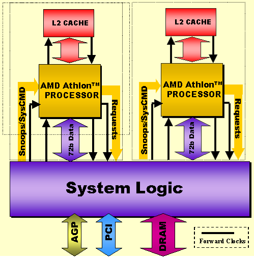
The EV6 bus protocol is scalable from 200MHz to 400MHz (100MHz x 2 - 200MHz x 2), with the next logical step being the 266MHz (133MHz x 2) FSB frequency. At 266MHz the EV6 bus provides 2.13GB/s of bandwidth, and at 400MHz the bus offers a whopping 3.2GB/s of bandwidth. The key to EV6's success isn't the high operating frequency, but the expandability and flexibility it offers as a solution. GTL+ is easily saturated, and EV6 is the answer.
Athlon's Architecture
As briefly mentioned before, the Athlon is the first 7th generation x86 processor to hit the streets according to AMD. The key to the Athlon's success is the ability to do more at the same time than any currently available Intel processor. The language of x86 can be defined as the x86 instruction set, however each x86 processor has a different way of interpreting this universal language, sort of like how different dialects can interpret similar words differently.
AMD Athlon Block Diagram (Click to Enlarge)

The P6 core, which is the base of the Pentium III albeit originally introduced in 1996 with the Pentium Pro, takes the instructions it receives and decodes them into (sometimes) smaller operations. The theory behind this is that it is much easier to tackle a problem if it is split up into multiple smaller parts. Why? Because unlike the conventional thinking we are used to, processors are capable of completing multiple tasks simultaneously, which is the key to their success.
| Both the Athlon and P6 (Pentium III) core are capable of decoding three instructions simultaneously, however in the case of the P6, the decoders cannot accept 3 complex instructions and process them simultaneously. In the case of the Athlon, regardless of the nature of the instructions, the decoding units are capable of decoding three instructions, regardless of nature, simultaneously. | 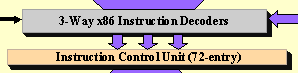 |
Another point of improvement the Athlon offers over Intel's P6 core (yes, you read that right, AMD is not only going for competitive performance but they are looking to surpass Intel) is the accuracy of the processor's branch tree prediction. We've all met individuals that are undoubtedly predictable in life, whether it's because of something they always say or do, our minds get used to expecting a certain type of behavior from them when placed in a specific set of circumstances. The same applies to the Athlon, whose 2048-entry branch prediction table takes on the task of storing commonly used operations and attempts to predict what the next operation to come down the pipeline will be. Not only is the table 4 times as large as Intel's branch prediction table, but in the event that the Athlon incorrectly "guesses" at what the next operation will be, the penalty isn't as great as that of the P6 core. This is simply because of the Athlon's shorter pipelines (10-stage integer and 15-stage FP pipelines vs 15-stage integer and ~30-stage FP pipelines for the P6 core) which make sure that the Athlon doesn't have to start from scratch after a missed prediction.
| The original debates (the politically correct way of saying flame wars) over the topic of AMD's FPU that occurred in newsgroups and online forums everywhere criticized both AMD and Cyrix FPUs for being poor performers in comparison to Intel. At the time, the most commonly used buzzword when backing that statement up was that Intel had a fully pipelined FPU and the rest didn't. | 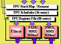 |
The argument no longer stands for AMD, as the Athlon's low latency FPU is now fully pipelined and is thus a definite competitor to Intel in terms of raw FPU performance. Athlon users won't have to worry about whether or not a game is 3DNow! optimized to get the most performance out of it.
Enhanced 3DNow!
AMD worked very closely with Microsoft as well as graphics card manufacturers to make sure that support for their Athlon was placed in Windows 98 SE and graphics card drivers. The support is not only for optimizing applications for the core of the Athlon, but also for the Athlon's Enhanced 3DNow! instruction set.
If you recall from the discussions earlier, 3DNow! brought SIMD execution to floating point operations that helped mask the weakness of the K6-2 and K6-III FPUs by providing an elegant way of improving performance. Those 21 instructions drew quite a bit of attention since their original implementation in 1998 and now have a very strong following in terms of support in games and in video drivers. The Athlon takes advantage of those 21 original instructions and adds 24 new instructions.
AMD included support for 19 new instructions that mimic the cache and streaming controls of Intel's SSE instructions, even using the same opcodes to maintain a level of compatibility between the two implementations. The cache and streaming controls are designed to help alleviate the effects of memory latency resulting from stalling the CPU pipeline.
The 5 remaining instructions that were added in for the Enhanced 3DNow! of the Athlon are digital signal processing extensions for soft modems, soft ADSL, complex math, MP3 and Dolby Digital decoding. Although the true performance benefits of the DSP extensions cannot be fully seen until implemented, the direction of such a move for AMD is definitely a positive one.
For the K6-2, 3DNow! offered a huge improvement in performance simply due to the lackluster performance of the K6-2's FPU however with the Athlon, this is not the case. The Athlon's FPU is already incredibly advanced and a very strong performer, and the effects of the Enhanced 3DNow! optimizations are essentially equal to the effects of SSE on the Pentium III, meaning that the improvement is there, just not as noticeable as with the K6-2.
As far as software/OS support goes, Microsoft's Windows 98 SE and DirectX 6.2 take advantage of the Athlon specific optimizations, including support for Enhanced 3DNow!
The Chipsets
The current chipset used to drive the Athlon is the AMD 750 chipset. The 750 is very similar to the Intel 440BX in the sense that it supports a 100MHz memory bus, AGP 2X, Ultra ATA 33/66, and a handful of the basic features that BX motherboard owners have come to expect.
The main difference is obviously that the 750 supports a connection to the EV6 bus protocol instead of the GTL+ used by the BX chipset, and unfortunately the 750 only supports single processor configurations which won't truly take advantage of the EV6 bus.
ALi, SiS, and VIA have already announced that they will be working on solutions for the Athlon due out either later this year or early in 2000. The VIA solution will be the one to look out for, sources close to VIA have indicated that their Athlon chipset will support AGP 4X transfer modes, PC133, Ultra ATA 66, but will still be for uni-processor systems only. ALi and SiS should have competitive solutions as well, but if history has taught us anything, we should expect at least one low cost Athlon chipset to emerge for the users that want the performance without all of the frills.
While AMD has been boasting support for multiprocessor Athlon setups, the question no one seems to ask is where are the multiprocessor chipsets and motherboards? Making a multiprocessor chipset and motherboard is extremely difficult, especially for manufacturers that have never done it before. AMD is hinting at next year for the first dual processor Athlon systems, however the chipsets that will support it are currently not in existence. Keep your eyes open for what happens there, it should be very interesting.
AGP Miniport Drivers
Remember the wonderful AGP miniport drivers for Super7 chipsets? Don't worry, the AMD 750's miniport is nowhere near as bad as the older VIA/ALi drivers which is a very good thing, however how compatible is the 750 with current generation AGP cards?
For those of you that think that only AMD owners have to use AGP GART drivers you're misinforming yourself, Intel LX/BX owners need them too. The only difference is that the drivers for Intel's implementation of the AGP Graphics Addressing and Remapping Table are built in to Windows 98 and therefore you don't need to load any drivers externally.
Unfortunately, AMD does not have the same luxury, and they must have their AGP GART miniport drivers installed for true compatibility. The drivers are currently at revision 4.45, the drivers that shipped with the Athlon review systems was revision 4.41 and the drivers we used were revision 4.44. The only differences between the three are minor performance tweaks, and some compatibility issues.
So here's the big question, can you use an Athlon with a TNT2? Yes. A G400? Yes. All other current AGP 2X cards? Yes. What about the NV10 and 3dfx's next-generation product? You can never say for sure, but it would be very unexpected if they didn't work with the AMD 750 or other Athlon chipsets using the latest AGP GART drivers.
The performance of the drivers is still not up to their full potential, but even with the drivers operating at their current level of performance the Athlon packs quite a punch.
The Motherboards
| The motherboards that AMD shipped
to reviewers with the Athlon 600s were the AMD Fester Rev. B boards that AMD developed in
house, but can you buy them? No. So what motherboards will you be able to buy? AMD's Fester Motherboard (right) |

| Gigabyte's GA-7IX and Microstar's
MS-6167 will be among the first available boards, both will boast 5 PCI slots, 2 ISA
slots, and the rest of the features supported by the AMD 750 chipset. The FIC SD11 is also
on its way, however information on that particular model has been kept very quiet. If
history repeats itself, FIC's excellent relationship with VIA should surface once again
with FIC being the first motherboard manufacturer to showcase a VIA chipset based Athlon
motherboard, possibly later this year. Gigabyte's GA-7IX Motherboard (right) |
The motherboard situation with the Athlon processor will be an interesting one. If you recall, one of the major problems with the Super7 market was the lack of high quality motherboards to drive the chips that AMD had spent so long producing. Motherboard manufacturers will hopefully take the Athlon a bit more seriously now that it is a top tier performer. Our current experience with Athlon motherboards in AnandTech's lab indicates that the manufacturers have a bit of work to do before we get the quality of the mainstream BX boards in the AMD 750 based Athlon motherboard solutions.
The Athlon draws a considerable amount of current, and thus the reference AMD motherboard features a set of voltage regulators alongside the Slot-A connector in order to supply the Athlon with the current it needs, when it needs it. Although the core voltage of the Athlon is lower than the Pentium III at 1.6v, the amount of current the powerful processor draws makes the quality of the motherboard it is installed on a very important issue to take into consideration. At the same time, we noticed some stability problems with some TNT2 Ultra cards and the Athlon, especially in cases where the TNT2 Ultra was drawing more than 5A of power. While these issues are certainly related to premature production of the motherboards (as they should, these motherboards are still in beta), they definitely need to be given some attention as it would be very unfortunate for the motherboard situation to hurt the Athlon.
Overclocking: How it's done
The question most of you are probably asking now (in addition to "how well does it perform?") is, can it be overclocked?
The answer is yes. AMD, from the start, has not had any intention of providing a multiplier lock on their processors, however they are very concerned with remarking. The K6 processor was one of the easiest chips to remark, and later generations of the K6 family didn't make it much more difficult for remarkers to overclock and sell the processors at higher prices. The Athlon changes all that.
| If you take a look at the Athlon's processor card, you'll notice that in the upper right hand corner there is a connector. That connector is the key to overclocking the Athlon. A controller module featuring dip-switches is plugged directly onto the connector and using that you can set the clock multiplier of the Athlon processor. | 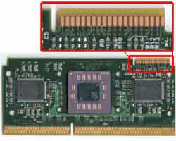 |
Once the clock multiplier is reprogrammed, you can remove the controller and go about using your chip normally. This unfortunately means that you have to remove the Athlon CPU from its casing, which will void all warrantees (but so does overclocking, so it's not that big of a loss). You'll just want to make sure that you don't damage the processor while removing the external casing.
Unfortunately the controller chips are very difficult to come by, a few manufacturers have them in their possession and they're present in AMD's labs as well as a few other places, but generally speaking, they're not easy to come by. The data sheets on that particular connector have yet to be released, but don't be surprised if they get leaked to certain Taiwanese motherboard manufacturers and you begin seeing overclocking controllers appear in the market, sort of like Socket-370 to Slot-1 Sloket adapters that allow for dual processor operation.
Overclocking: The Results
So how far can these things be pushed? Kryotech was the first to show off an overclocked Athlon with their Super-G system at 1000MHz. Unfortunately the 1000MHz systems won't be out until later this year, the systems that will first be available will be the Cool Athlon 800s running at, you guessed it, 800MHz. The Cool Athlon 800s will make use of the 650MHz Athlon processor, thermally accelerated (aka overclocked) to 800MHz. But how far can you get without the extreme Kryotech cooling?
Although we can't quote you definite clock speeds as each chip will most likely overclock to a different extent, 700MHz out of a 650MHz chip isn't too far fetched of a goal, and obtaining a 750MHz overclock is more realistic than you'd think… ;)
The Test
AnandTech's Slot-A test system was configured as follows
- AMD Fester Motherboard Revision B
- Gigabyte 7IX Motherboard Revision 0.7
- AMD Athlon 600 & 650
- 128MB SDRAM
- 22GB IBM Ultra ATA 66 HDD
- 3dfx Voodoo3 3500TV clocked at 183/183MHz for all 3dfx tests
- Diamond Viper V770 Ultra clocked at 150/183MHz for all NVIDIA tests using Detonator 2.08 drivers
- Matrox Millennium G400MAX clocked at 166/200MHz for all Matrox tests
- AMD 750 AGP GART drivers version 4.44
AnandTech's Slot-1 test system was configured identically except for the motherboard and CPU which were as follows:
- ABIT BE6
- Intel Pentium III clocked at 650, 600, 550, 500, 450
- Intel Pentium II clocked at 400, 350, 333, 300, 266, 233
- Intel Celeron clocked at 500
AnandTech's Super7 test system was configured identically except for the motherboard and CPU which were as follows:
- Tyan Trinity S1598
- AMD K6-III clocked at 450MHz
- AMD K6-2 clocked at 450MHz
All benchmarks were run at 1024 x 768 x 16-bit color unless otherwise specified.
Quake 3 Arena Test Settings
The four different image quality settings for Quake 3 Arena Test were Fastest, Fast, Normal and High using q3demo1.dm3. To run the test, bring down the console by hitting '~' then type in 'timedemo 1' then hit return and type 'demo q3demo1' and hit return.
Screenshots of the four settings are provided below:
Click to Enlarge
Fastest Setting

Fast Setting

Normal Setting

High Setting

Business Application Performance
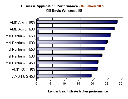
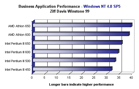
Business Winstone 99 has become an unspoken requirement for benchmarking here at AnandTech, and as you can see below, the Athlon simply dominates over the Pentium III. Even when clocked at 650MHz, the Pentium III has a bit of climbing to do before it can even reach the Athlon at 600MHz, being around 5% slower although it boasts a 50MHz clock speed advantage. Only the Athlon at 500MHz would be slower than the 650, with the 550MHz Athlon being about on par with the Pentium III 650.
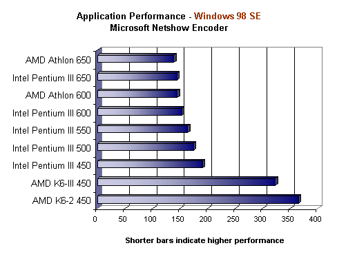
Intel's supplied us with a Microsoft Netshow Encoder benchmark that is supposed to take advantage of Intel's SSE. Even with the optimizations for the Pentium III's SSE instructions, the Athlon 650 and 600 still beat out their equivalently clocked Intel counterparts. It's funny to note that AMD also provided us with a Netshow benchmark, under which both Athlon processors dominated the score boards. It just goes to show you that with extreme optimizations, you can prove the Athlon slower or faster than the Pentium III. But in reality which is it? The Athlon is definitely not slower than the Pentium III, but the advantage it holds over the Pentium III varies depending on the application.
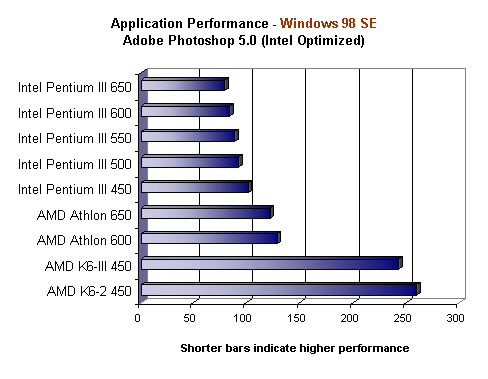
Once again, both Intel and AMD provided us with an Adobe Photoshop benchmark, the results? The Intel benchmark showed that the Pentium III was faster than the Athlon, and the AMD benchmark showed the exact opposite. How meaningful are the Photoshop benchmarks as well as others provided by either of the two CPU manufacturers? It depends on the level of SSE or 3DNow! optimizations present in the benchmark, the Photoshop benchmark below is obviously SSE optimized and AMD's Photoshop benchmark is obviously optimized for the Athlon so neither benchmark makes a good real world gauge of how fast the processors are.
The best measure of application performance still seems to be Winstone which makes no use of SSE or 3DNow! specific optimizations. The Photoshop benchmark is meaningless, regardless of whether it is the AMD or Intel version and unfortunately most benchmarks supplied by AMD and Intel carry the same biased optimizations. It is interesting to see the Athlon beat the Pentium III in an application specifically optimized for the Pentium III such as in the Netshow Encoder benchmark. At the same time, the Pentium III never beat the Athlon in a benchmark that was supposed to be optimized for the Athlon.
In terms of raw power, the Athlon is the faster chip, and in real world usage, our money is on the Athlon.
We used the NVIDIA TNT2 Ultra as the base graphics card for our gaming tests, but as you'll see later on we did repeat some of the tests using both the Voodoo3 3500TV and the Matrox G400 to eliminate any possible optimizations for one processor or another by the video card manufacturer.
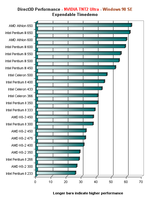
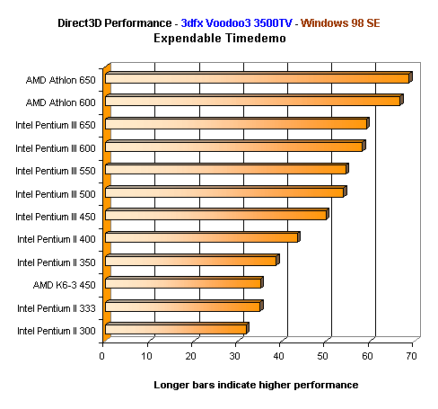
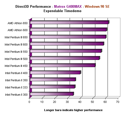
While reviewing video cards, coming up with a good real world Direct3D game benchmark is next to impossible. Shogo never produced representative results and Expendable was too CPU dependent to be a good measure of differences between graphics cards. Luckily, we're reviewing a CPU here, not a graphics card and Expendable quickly turns into the perfect benchmark.
Expendable on the TNT2 Ultra places the 650MHz Athlon at the top of the benchmarks list, followed closely by the Pentium III at 650MHz and then the Athlon at 600MHz. A 550MHz Athlon would be a little slower than a Pentium III 600 and a 500MHz Athlon should be around the speed of a Pentium III 550.
If you look down towards the end of the graph you can see where AMD has come from in terms of gaming performance since 1998.
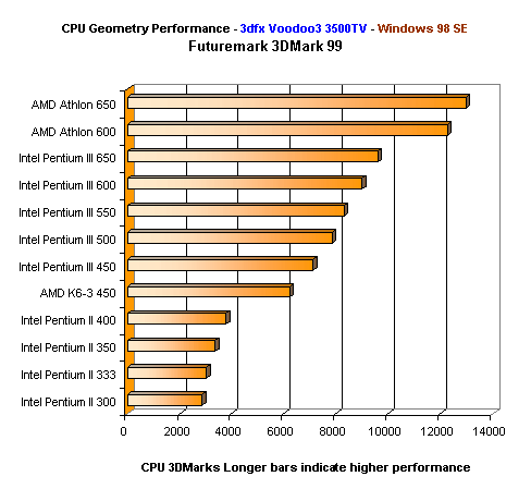
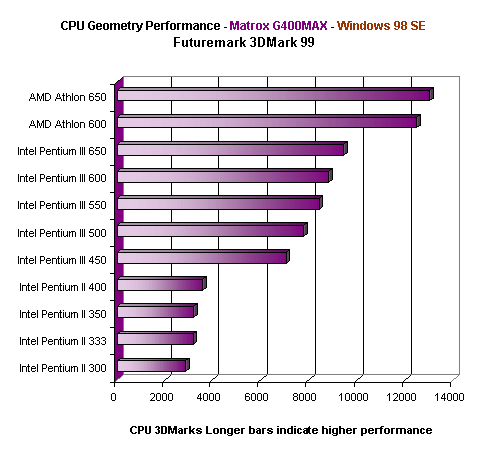
3DMark 99 offers an excellent way to benchmark the type of performance a particular video card will obtain from a CPU using the CPU Geometry Performance test measured in CPU 3DMarks. Both Athlons were using a Athlon specific 3DNow! DLL in the test, however using an unmodified copy of 3DMark still put both the Athlon 600 and 650 at levels greater than the fastest Pentium III in the test.
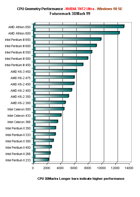
The results speak for themselves, the Athlon has the power to make it to the top of the market, but will it? Let's move on...
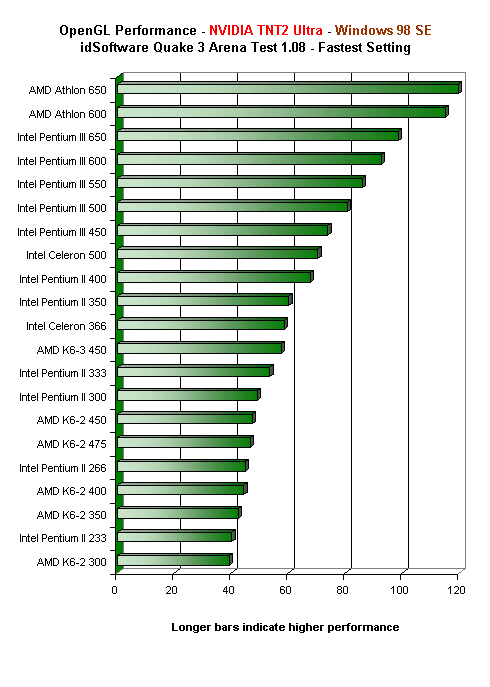
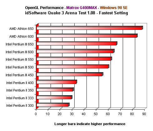
idSoftware's Quake 3 Arena Test is another wonderful CPU test because it offers four built in image quality settings which stress the CPU in different ways. The Fastest and Fast settings allow the CPU to take over and push the graphics card to its limits at lower resolutions, the Normal setting provides for a simulation of average gameplay, and the High setting gives us an indication of the limits of the graphics card.
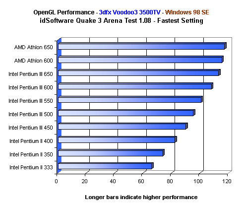
The fastest image quality setting gives us an indication of what the CPU is capable of doing, and as you can tell from the below chart, as the only processor breaking the 100 fps barrier, the Athlon 600 and 650 bring gamers back to the AMD name. Only a 700MHz Pentium III could potentially threaten the 600MHz Athlon, and for a gamer that can't afford the 600, the Athlon 500 should do just fine and offer performance comparable to that of at least a Pentium III 600 if not greater.
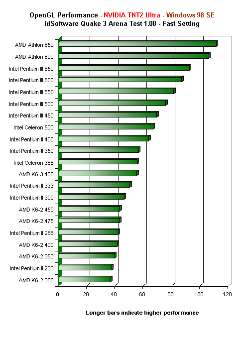
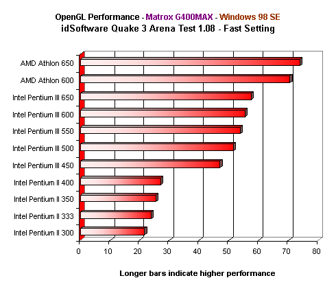
The results of the benchmarks at the fast image quality setting almost mirror those run at the fastest setting, although the gap between the Athlon 600 and the Pentium III 650 does begin to close as the TNT2 slowly exhibits fill rate limited behavior.
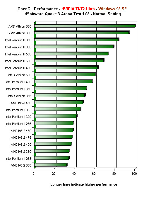
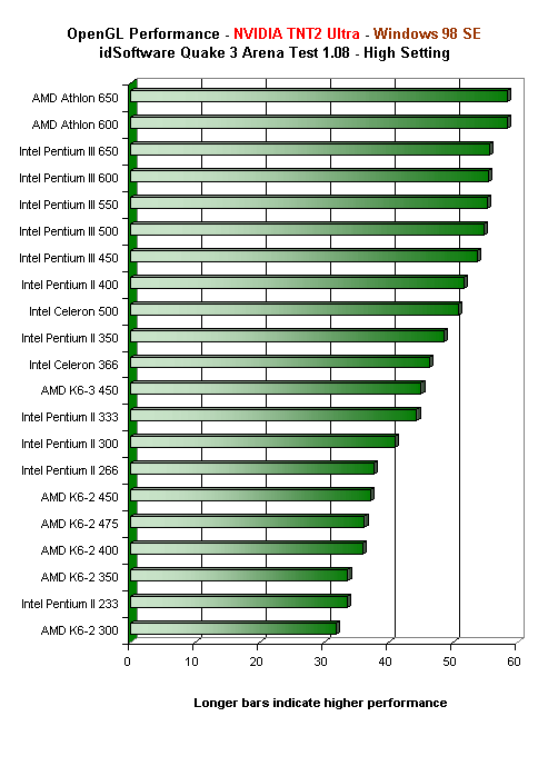
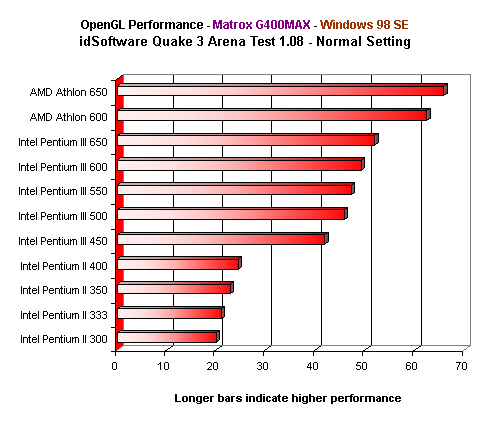
AMD continues to keep a healthy lead over the competition even at the normal image quality setting. Even for the hardcore gamers, the Athlon is a very viable solution.
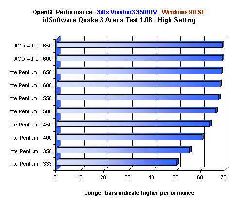
Hitting the limits of the TNT2 Ultra, the Athlon 650 still keeps the lead over the Pentium III at 650 which still can't beat the Athlon at a slower 600MHz clock.
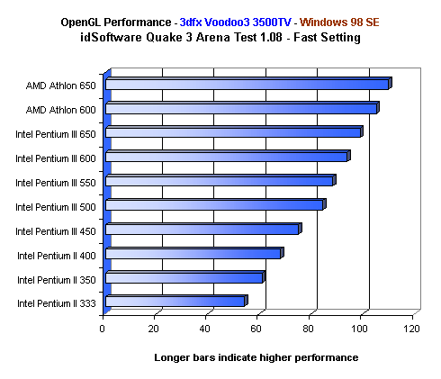
With a Voodoo3 3500 the results are very similar to the TNT2 Ultra tests, except in expendable, the Pentium III at 650 doesn't come near to beating the Athlon at 600MHz.
The fastest setting on the 3500TV test bed gave the Pentium III 650 a chance to play catch up with the Athlon 600, but still didn't have what it takes to beat AMD in the benchmark. Just 6 months ago you would've never expected to see AMD make this big of a performance impression on the market.
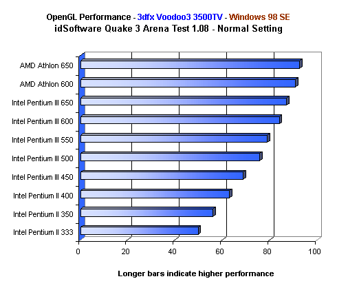
Nothing new here, the Athlon keeps the lead all the way through to the end.
The G400MAX, a very CPU dependent graphics chip, had no problem appreciating the raw power of the Athlon as you can see from the graphs below.
OpenGL had been a very weak facet of the G400's performance, even the G400MAX didn't perform all that well in OpenGL applications. But if you look at the graph below you'll see where the Athlon picks up and shows the Pentium III what the G400MAX is really made of.
The trend continues even in the Fast and Normal settings, the Pentium III at 650MHz doesn't come close to touching the Athlon at 600. With the G400MAX it would take a slower 500MHz Athlon before the Pentium III could even catch up at 650MHz.
Windows NT Performance
Ever since the release of the K6-3, AMD has been a strong performer in NT so long as the tasks didn't involve many FPU intensive applications. As you can see by the Business Winstone 99 benchmarks, the Athlon still keeps that flame alive but adds something new...
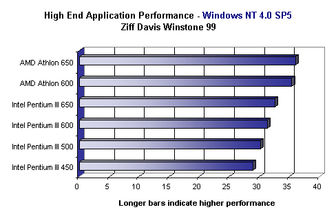
...not only does the Athlon dominate in Business Application performance, but in High End application performance as well, courtesy of its strong FPU. Once again, another statement we'd never think you'd hear just 6 months ago.
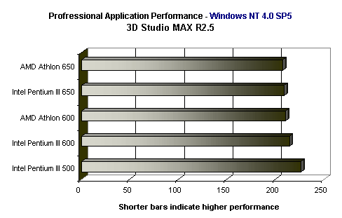
Using Kinetix's own 3D Studio MAX benchmark (bundled with 3D Studio MAX R2.5, just run the MAXScript bench.ms) the Pentium III and Athlon become close performing partners, with the Athlon just edging out above the Pentium III in terms of performance clock for clock.
Final Words
I don't have to give you a conclusion here, the benchmarks speak for themselves, the Athlon is the fastest desktop x86 processor on the market. It would take at least a 700MHz Pentium III to start to beat AMD's Athlon, but even if Intel does release a Pentium III 700 ahead of schedule, the price of a lower clocked but faster Athlon will still be lower than a 700MHz Pentium III. There is nothing in Intel's current family of processors that can match the performance of the Athlon, even the forthcoming Coppermine will have trouble competing against AMD's latest flagship.
Intel will most likely try to turn this into a price war of sorts, by driving the prices of the Pentium III and Celerons even lower Intel will hope to force AMD to do the same. As a company, AMD can't afford to get into a heated price war for long periods of time with Intel. Being the larger company, Intel can last longer in a price war than AMD can, thus for AMD, a price war is not the ideal situation for the Athlon.
Keep in mind that AMD has a much larger low end product line than Intel, while Intel has the Celeron, AMD now has the K6-III and K6-2 to play around with when it comes to keeping prices competitive. The K6-III is no longer the flagship, and therefore doesn't have to be priced as one. It should be interesting to see what Intel comes up with in retaliation to the Athlon, but whatever it is, don't expect to see it anytime this year. Intel may be able to push higher clock speeds than AMD in 1999, but as far as performance goes, it'll take much more than a Coppermine to beat the Athlon.
Just because the Athlon is finally out the door doesn't mean that AMD will stop moving forward, they've got quite a bit in the works and they're definitely not going to stand idle while Intel tries to regain the lead as they've done in the past.
In the present time, AMD has the lead and Intel should be going back to the drawing board to rethink their approach towards competing with AMD. But when can you buy an Athlon? After talking to a number of vendors, the biggest complaint seems to be that companies like Compaq are buying up all the Athlons. The earliest you'll be able to go out and order an Athlon online seems to be in about two weeks, however that time frame is by no means a guarantee. In the past, AMD has had a number of problems delivering on their promises, this time, the performance is there, and if AMD can't deliver this part, it may be their last.
Luckily the news seems to be good so far, yields on the Athlon aren't great, but they're not poor. Assuming AMD can deliver on the demand for the Athlon (OEMs will start advertising Athlon based systems starting August 16, 1999), the next question is who will make the motherboards? Until recently, there haven't been many decent quality boards for non-Intel platforms, the Super7 market is the perfect example of that. Our first in lab experiences with Athlon boards haven't been pleasant and we can only hope that the right motherboard manufacturers will step up and support the Athlon.
AMD has finally made a chip that takes us all back to the days of the 386, when Intel wasn't the chip giant they are now, and AMD was the maturing company on the rise. Once again, kudos to AMD for a job well done, but the game isn't over yet, not by a long shot...
The Future of the Athlon