
Original Link: https://www.anandtech.com/show/1541
FIRST LOOK - nForce4: Gigabyte K8NXP-9
by Wesley Fink on November 12, 2004 8:00 PM EST- Posted in
- Motherboards
It has been just a few weeks since nVidia launched their nForce4 chipset - their first chipset with PCI Express for Athlon 64. Rumors have abounded since that launch that the nForce 4 might be delayed due to issues with the 1000 Hyper Transport of the nF4 chipset. We had also been told by several manufacturers that companies like Asus, MSI, and Gigabyte - often called the Tier 1 manufacturers - would be the first to launch both nForce4 and the SLI version of nForce4 for dual nVidia video cards. This would be followed a few weeks later by nForce4 boards from smaller manufacturers.
While we have speculated as to who might be first to market with nForce4, we are pleased that this is no longer a mystery. Gigabyte is the first to get a production nForce4 board in our hands. The board itself arrived as a complete K8NXP-9 package, but the outside packaging was not ready when Gigabyte shipped the board to us from Taiwan. Other than the outside package and a limited early BIOS, the board is a production board.
We couldn't wait to run the production K8NXP-9 through our benchmarks, so we decided to do a "First Look" to bring you the news as fast as possible. We were also very interested in testing the performance and stability of the Gigabyte nForce4 compared to the nF4 Reference board. Our review of the earlier Gigabyte K8NSNXP-939, based on the nForce3 Ultra, did not find it to be one of the top boards in our Socket 939 Roundup: Battle at the Top. Have things improved? There have also been many end users who have reported issues with memory on the earlier Gigabyte nF3 Ultra board, so we wanted to see if that area had also improved in the nForce4 update.
Basic Features
| Gigabyte K8NXP-9 Specifications | |
| CPU Interface | Socket 939 Athlon 64 |
| Chipset | nVidia nForce 4 Ultra (Single-Chip) |
| Bus Speeds | 200MHz to 400MHz* |
| PCI Express Speeds | None in Pre-Release BIOS* |
| Core Voltage | 0.8V to 1.7V in 0.025V increments |
| CPU Clock Multiplier | 6x-25x in 1X increments* |
| HyperTransport Frequency | 1000MHz (1GHz) |
| HyperTransport Multiplier | 1X, 2X, 3X, 4X, 5X |
| DRAM Voltage | 2.5V to 3.1V in 0.1V increments* |
| HyperTransport Voltage | Normal, + 0.1V, +0.2V, +0.3V |
| Memory Slots | Four 184-pin DDR DIMM Slots Dual-Channel Configuration Regular Unbuffered Memory to 4GB Total |
| Expansion Slots | 1 x16 PCIe Slot 2 x1 PCIe Slots 3 PCI Slots |
| Onboard SATA/SATA RAID | 8 SATA Drive Total 4 SATA 300 Drives by nForce4 (RAID 0, 1, 0+1, JBOD) Can be combined with IDE drives in RAID 4 SATA 150 Drives by Sil3114CT176 (RAID 0, 1, 0+1, JBOD) |
| Onboard IDE/IDE RAID | Two Standard ATA133/100/66 (4 drives) Drives may be as IDE RAID or combined with nF4 SATA drives in a RAID Array |
| Onboard USB 2.0/IEEE-1394 | 10 USB 2.0 ports supported by nForce4 2 Firewire 1394B by TI 46A9C3W |
| Onboard LAN | Dual Gigabit LAN On-chip Gigabit LAN by nF4/Cicada 8201 PHY PCI Express Gigabit LAN by Marvel 88E8053 |
| Wireless LAN | PCI 802.11b/g Wireless LAN Card Included |
| Onboard Audio | AC '97 2.3 8-Channel by Realtek ALC850 |
| BIOS Revision | Award GA-K8NXP-9 M01 11/02/2004 |
The shipping Gigabyte BIOS provided many of the options that you would expect on a top-line board, but several areas like clock frequencies, memory voltage, and CPU ratios were very limited in the pre-release BIOS. The values reported in the chart above are the values that Gigabyte has assured us will be available in the production BIOS. These are much better ranges than those seen on recent Gigabyte boards. Most Enthusiasts will find these ranges very useful in tweaking the Gigabyte for top performance. As is Gigabyte custom in recent designs, Advanced Chipset Features (and Memory Timings) can only be seen when you press CTRL+F1 while in the BIOS.
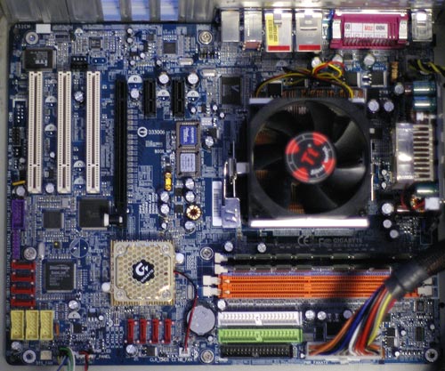
The Gigabyte K8NXP-9 was designed as a top-of-the-line nForce4 motherboard. As the flagship model, it sports all the top Gigabyte features. This starts with the DPS daughter card that you can see on the right of the board picture. This is used to increase power reserves and stability by increasing the board to 6-phase power. You will also see dual BIOS chips to the right of the PCIe x16 video slot. This trademark Gigabyte feature provides back-up BIOS in the event of a bad flash or unstable BIOS setting. The K8NXP-E can boot from the good backup BIOS if problems arise with the main BIOS.
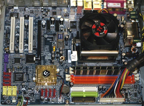
An analysis of board layout is beyond the scope of a First Look, but there are several things that stand out on the Gigabyte. Power connectors are ideally located on board edges in reasonable locations. This will be appreciated by anyone who has tried to snake these bulky cables around a CPU or fan. The floppy and IDE connectors are also ideally located on the far right edge of the board above the midline. Ports are concentrated at the bottom of the board, out of the way of the PCI and PCIe slots.
Continuing the theme of "more than you might expect", Gigabyte provides eight SATA ports. Four ports are 3Gb/s ports provided by the nForce4 chip, and four ports are 1.5Gb/s ports driven by the PCI bus. The 2nd group of ports is useful, but they would have been much more exciting if they had been 3Gb/s ports like those provided by nForce4.
Probably the most significant upgrade from the nF3 Ultra Gigabyte is the decision to adhere to nVidia's feature set. This time, we see Gigabyte use the nF4 on-chip Gigabit LAN by supporting it with a Vitesse (Cicada) Gigabit PHY. In fact, Gigabyte went one step further by including a second Gigabit LAN on the PCI Express Bus. This second on-board LAN is also removed from the constraints of the slower PCI bus since it resides on the much faster PCIe bus. For those using wireless networks there is a even a third option as Gigabyte includes a PCI 802.11 b/g card in the package.

Audio is AC '97 2.3, but Gigabyte uses the popular 8-channel Realtek ALC850. The K8NXP-9 includes a wide range of audio I/O to make the most of the 850 chip. This includes 6 programmable audio mini-jacks and coax SPDIF in and out - all on the rear panel. There is more information on the Realtek 850 at the Realtek web site for those who are interested.
Another pioneering feature for Gigabyte has been their support of 1394B Firewire on their boards. This continues with the K8NXP-9 with 2 ports capable of 800MB/s. This is double the speed of 1394A for those looking for fast Firewire access.
Overclocking and Memory Stress Testing
With the limited ranges of CPU clock speeds available in the pre-release Gigabyte BIOS, it was not possible to test overclocking thoroughly. We were able to reduce multipliers and easily reach 250FSB, which was the top speed available in the pre-release BIOS. However, until we receive the updated BIOS, we cannot determine the full overclocking capabilities of the K8NXP-9.Since there have been many reports of issues with memory on the earlier Gigabyte nForce3 Ultra, more effort went into testing memory performance on the K8NXP-9. Our memory stress test measures the ability of the K8NXP-9 to operate at its officially supported memory frequency (400MHz DDR), at the lowest memory timings that OCZ PC3200 Platinum Rev. 2 modules will support. All DIMMs used for stress testing were 512MB double-sided (or double-bank) memory. To make sure that memory performed properly in Dual-Channel mode, memory was only tested using either one dual-channel (2 DIMMs) or 2 dual-channels (4 DIMMs).
| Stable DDR400 Timings - One Dual-Channel (2/4 DIMMs populated) |
|
| Clock Speed: | 200MHz |
| CAS Latency: | 2.0 |
| RAS to CAS Delay: | 2T |
| RAS Precharge: | 10T* |
| Precharge Delay: | 2T |
| Command Rate: | 1T |
Using two DIMMs in Dual-Channel 128-bit mode, the memory performed in all benchmarks at the fastest 2-2-2-10 timings, at default voltage. As a further test, we ran every pair of PC3200 DIMMs that we had in the lab at their fastest timings, at DDR400 in DC mode. We had no problem with any RAM that we tested. It appears that the problems with Dual-Channel mode and memory compatibility, which were reported on the earlier Gigabyte nF3 Ultra board, have been improved greatly or eliminated on this nForce4 version.
| Stable DDR400 Timings - 4 DIMMs (4/4 DIMMs populated) |
|
| Clock Speed: | 200MHz |
| CAS Latency: | 2.0 |
| RAS to CAS Delay: | 2T |
| RAS Precharge: | 10T* |
| Precharge Delay: | 2T |
| Command Rate: | 2T |
Tests with all four DIMM slots populated on the Gigabyte required a 2T Command Rate with 4 DIMMs in two dual channels. This is the pattern seen on other top-performing Socket 939 boards. However, an "Auto" setting for Command Rate would not boot, and we had to force a 2T setting in BIOS with 4 DIMMs. Once 2T was set in BIOS, there was no problem running 4 DS DIMMs at the same aggressive 2-2-2-10 timings we had used with 2 DIMMs.
Test Setup
The performance of the Gigabyte K8NXP-9 was compared to the nVidia nForce4 Reference board using an AMD FX55 and 2-2-2-10 DDR memory. Test results with the Intel 925XE Abit Fatal1ty AA8XE were included for Reference with the fastest 1066FSB CPU currently available. For reference, test results were also included for the Intel 925X with the 560 - the fastest current Intel 800FSB CPU. All benchmarks on all platforms were run with the PCI Express nVidia 6800 Ultra. Tests on the Gigabyte K8NXP-9 were all run with 5X (1000 HT) enabled.| Performance Test Configuration | |
| Processor(s): | AMD Athlon 64 FX55 (2.6GHz-1MB Cache) Socket 939 AMD Athlon 64 4000+ (2.4GHz-1MB Cache) Intel 3.46EE (1066FSB) Intel 560 (3.6GHz 800FSB) |
| RAM: | 2 x 512MB OCZ PC3200 Platinum Rev. 2 2 X 512MB Micron DDR2-533 |
| Hard Drive(s): | Seagate 120GB 7200 RPM IDE (8MB Buffer) |
| Chipset Drivers: | nVidia nForce 6.31 Beta (nForce4) |
| Video Card(s): | nVidia 6800 Ultra (PCI Express) |
| Video Drivers: | nVidia nForce 61.81 Beta |
| Operating System(s): | Windows XP Professional SP1 |
| Motherboards: | Gigabyte K8NXP-9 (nForce4) nVidia nForce4 Ultra Reference Board Abit Fatality AA8XE (Intel 925XE) Intel 925X Reference Board5 |
The configuration was kept as close as possible between the 4 motherboards, but we are forced to compare apples to oranges in some cases. DDR400 memory at 2-2-2-10 is being compared on the nForce4 boards to DDR2-533 at 3-3-3-10 on the Intel 925X/XE boards. However, as we saw in the DDR vs. DDR2 review, the performance of fast DDR400 and DDR533 is very close.
Performance Tests
DirectX 9 Gaming
There were many positive responses to using a larger group of DirectX 9 games in our last "First Look", so we're including more recent DX9 games in this "First Look" at a production nForce4 board.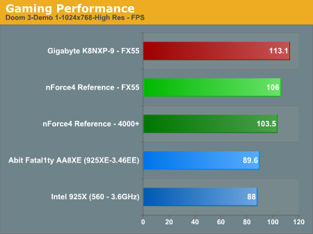
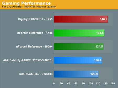
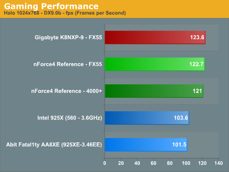
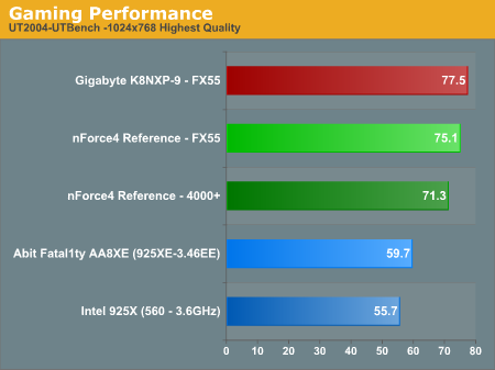
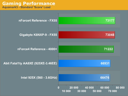
The real comparison here is the nVidia nForce4 Reference Board and the Gigabyte K8NXP-9. Gigabyte has done an excellent job on their nForce4 board. The K8NXP-9 wins every comparison with the nF4 Reference board except Aquamark 3, which is virtually the same with both boards. If this is a reflection of what is coming with shipping nF4 boards, we all have reasons to be pleased. For now, it is fair to say that the Gigabyte K8NXP-9 provides the best performance we have seen on an nForce4 motherboard
Performance Tests (Continued)
DirectX 8 & OpenGL Gaming

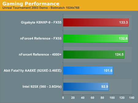
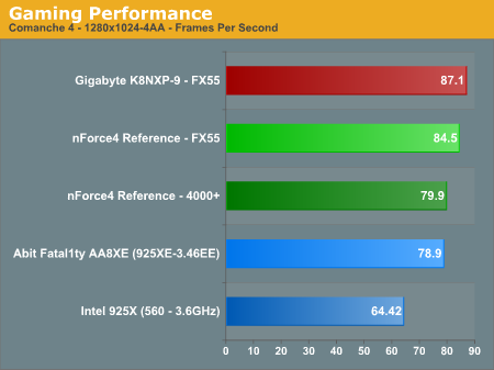
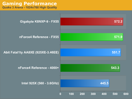
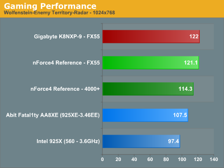
The pattern continues on DX8 and Open GL, with the K8NXP-9 topping the charts in every game benchmark. This is what we would expect in shipping boards compared to the Reference boards on which they are based. More often than not, however, the Reference Board retains the performance lead. Gigabyte did a very good job of tweaking the performance of this nForce4 board.
General Performance
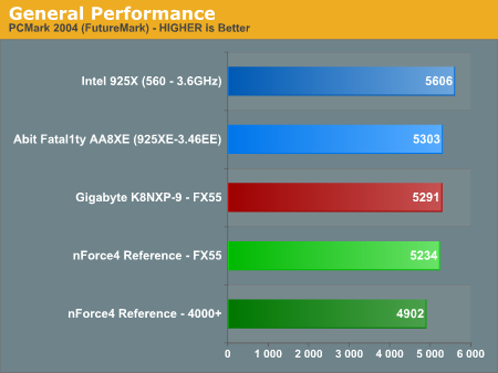
Intel normally tops the PCMark 2004 benchmarks, as they do in Sysmark, which is also produced by Future Mark. This is one of the few remaining benchmarks where Intel is the usual winner. This is likely the result of code optimizations for Intel features, and even this advantage may change when the Rev. E Athlon 64 chips appear with SSE3 code. The Gigabyte is still a bit better in performance than the nForce4 Reference board.
Our Take
In this First Look at the Gigabyte K8NXP-9, we come away very impressed with the features and performance of the first shipping nForce4 board. We have been a critic recently of Gigabyte adding everything but the kitchen sink to their top-of-the-line boards. This is because the features often made no sense at all, being little more than "check-list" items. As an example of this, Gigabyte did not implement the nVidia on-chip Gigabit LAN on their nForce3 Ultra board and instead, substituted a PCI LAN chip. Recently, Gigabyte boards have seemed to be more of a checklist of what you could add to a board instead of a thoughtfully engineered product, such as we had come to expect from Gigabyte.This go-around, it is very clear that Gigabyte has given much more thought to the board design. The added features actually make sense on the K8NXP-9 as part of the whole board. Particularly noteworthy is Gigabyte's decision to include dual Gigabit LAN on their nForce 4 - one an on-chip PHY, and the other on the PCIe bus. We are also happy to see the continued support of 1394B high-speed Firewire, the 6-phase daughter card and the dual BIOS. The only frivolous extra that we see is the 1.5Gb SATA when the nForce4 provides 3Gb SATA, but we could even argue that this is a positive feature if the Silicon Image controller supported peripherals other than hard drives. Overall, Gigabyte has done a very good job with the feature set of the K8NXP-9. It's about time.
It is hard to argue with the excellent stock performance of the K8NXP-9 as it simply tops almost every benchmark compared to nF4 Reference. The memory performance, a very sore spot with the Gigabyte nF3 Ultra design, also seems very solid. This Gigabyte board was a joy to test and was exceptionally stable in all our benchmarks. It certainly appears that Gigabyte heard the litany of complaints about memory performance with the K8NSNXP-939 because the K8NXP-9 is both fast and stable with any memory that we threw at it.
The last area is overclocking or Enthusiast features. We were unfortunately not able to fully test the capabilities of the K8NXP-9 due to the limited Clock frequencies, memory voltage, and CPU ratios available in the pre-release BIOS. Gigabyte Engineers have given us ranges that they say will be included in production BIOS, which we have shared. As soon as the BIOS with expanded ranges is available, we will add an update to this review or include results in a future roundup. The ranges Gigabyte has committed to include will make many Enthusiasts happy. The expanded memory voltages, in particular, would be a first for Gigabyte. That feature will be welcomed indeed by memory overclockers.
It is too early to know if the Gigabyte K8NXP-9 is representative of a great group of nForce4 boards or if it is the standout of the group. For now, if Gigabyte comes through with the BIOS updates that they have promised, we can enthusiastically recommend the K8NXP-9. It's the first Gigabyte board in quite a while that I could comfortably run in my own personal rig, and that isn't faint praise.


