Original Link: https://www.anandtech.com/show/2116
NVIDIA's GeForce 8800 (G80): GPUs Re-architected for DirectX 10
by Anand Lal Shimpi & Derek Wilson on November 8, 2006 6:01 PM EST- Posted in
- GPUs
We always get very excited when we see a new GPU architecture come down the pipe from ATI or NVIDIA. For the past few years, we've really just been seeing reworked versions of old parts. NV40 evolved from NV30, G70 was just a step up from NV40, and the same is true with ATI as well. Fundamentally, not much has changed since the introduction of DX9 class hardware. But today, G80 ushers in a new class of GPU architecture that truly surpasses everything currently on the market. Changes like this only come along once every few years, so we will be sure to savor the joy that discovering a new architecture brings, and this one is big.
These massive architecture updates generally coincide with the release of a new DirectX, and guess what we've got? Thus we begin today's review not with discussions of pixel shaders and transistors, but about DirectX and what it will mean for the next-generation of graphics hardware, including G80.
DirectX 10
There has been quite a lot of talk about what DirectX 10 will bring to the table, and what we can expect from DX10 class hardware. Well, the hardware is finally here, but much like the situation we saw with the launch of ATI's Radeon 9700 Pro, the hardware precedes the new API. In the mean time, we can only look at our shiny new hardware as it performs under DX9. Of course, we will see full DX9 support, encompassing everything we've come to know and love about the current generation of hardware.
Even though we won't get to see any of the new features of DX10 and Shader Model 4.0, the performance of G80 will shine through due to its unified shader model. This will allow developers to do more with SM3.0 and DX9 while we all wait for the transition to DX10. In the mean time we will absolutely be able to talk about what the latest installment of Microsoft's pervasive graphics API will bring to the table.
More Efficient State and Object Management
One of the major performance improvements we will see from DX10 is a reduction in overhead. Under DX9, state change and draw calls are made quite often and can generate so much overhead that the API becomes the limiting factor in performance. With DX10, we will see the addition of state objects which hold all of the state information for a given pipeline stage. There are 5 state objects in DX10: InputLayout (vertex buffer layout), Sampler, Rasterizer, DepthStencil, and Blend. These objects can quickly change all state information without multiple calls to set the state per attribute.
Constant buffers have also been added to hold data for use in shader programs.
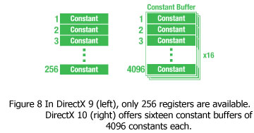
Each shader program has access to 16 buffers of 4096 constants. Each buffer can be updated in one function call. This hugely reduces the overhead of managing a lot of input for shader programs to use. Similar to constant buffers, texture arrays are also available in order to allow for much more data to be stored for use with a shader program. 512 equally sized textures can be stored in a texture array, and each shader is allowed 128 texture arrays (as opposed to 16 textures in DX9). The combination of 8Kx8K texture sizes with all this texture storage space will offer a huge boost in texturing ability to DX10 based games and hardware.
A new construct called a "view" is being introduced in DX10 which will allow resources to be used as more than one type of thing at the same time. For instance, a pixel shader could render vertex data to a texture, and then a vertex shader could use a view to interpret the data as vertex buffer. Views will basically give developers the ability to share resources between pipeline stages more easily.
There is also an DrawAuto call which can redraw an object without having to go back out to the CPU. This combined with predicated rendering should cut down on the overhead and performance impact of large numbers of draw calls currently being used in DX9.
Virtual Memory
Microsoft is taking tighter control of graphics memory with it's new driver model, and thus is able to provide virtual memory support for the graphics memory subsystem. What this means is that games no longer need to worry about running out of graphics memory. When software needs to write something to local memory, and local memory is full, Windows will be able to kick out something off the graphics card and put it in system memory (this is called paging) until it is needed. This happens without the software's intervention or knowledge. If system memory becomes full, data will be kicked out to the hard drive. Of course, if something like this happens the performance will definitely suffer.
Virtual memory isn't as much a performance enhancing tool as it is a way to remove the burden on the developer to manage memory usage around a hard limit of available space. Certainly, lots of paging will degrade performance, but lower performance is generally better than a crash. On the flip side, it is possible that virtual memory could increase performance by effectively replacing local graphics memory size with unused PCIe bandwidth. This has been the idea behind TurboCache and HyperMemory, but with the added advantage that the graphics driver doesn't need to worry about object or texture management between local and system memory.
Engineers have been wanting to see virtualized graphics memory for years, as operating on really huge data sets is made significantly easier when the software developer doesn't have to manage moving data in and out of graphics memory by hand. We've seen some limited benefits of utilizing both local and system memory on low memory TurboCache and HyperMemory cards. With game developers reaching towards ever larger data sets, high end parts will soon begin to benefit from virtualized graphics memory as well. Building the hardware to accommodate the possibility of higher latencies due to paging and allowing the OS to manage all the memory in the system will definitely help developers focus on building better games rather than better memory managers. That's not to say that memory management won't still be important to game developers. Making sure space and bandwidth are used efficiently are important factors in performance, but the ability to forget about hard limits in local memory will make it easier to take one efficient approach regardless of onboard memory.
Hardware Virtualization
Lately, all the big boys of computing have been infatuated with the idea of virtualization. It makes a whole lot of sense, really. With the advent of multi-core CPUs, AMD and Intel need to find ways to take full advantage of their processing power. Single thread execution time will never disappear as a factor in computing, and some algorithms just can't be parallelized.
Obviously, encouraging users to multitask is a simple way to provide a benefit to multi-core computing. The next step is to encourage developers to write highly multithreaded applications. Beyond that is to allow the user to run multiple operating systems on one set of hardware. One example of how this may be beneficial is in the use of a single system as a normal PC during its use as a home theater / DVR box. Another example is one we've already seen: Mac users running both Windows and OS X on Intel based Macs using a virtual machine manager like Parallels.
In order to really achieve the capabilities hardware providers would like to promote, more work must be done by hardware, software, and operating system providers. One of the major advances necessary is the virtualization of the graphics subsystem. With DirectX10 and the new WDDM (Windows Display Driver Model), graphics hardware is required to support virtualization. This is not a simple request, as games will no longer be guaranteed exclusive access to the hardware while running. We can potentially share game rendering with something like physics calculations on the same GPU. Or we could run a Folding@Home GPU client in the background while we play a game. On the extreme, multiple full screen 3d applications could be running concurrently.
Drivers and hardware will have to support context switching on a massive scale due the huge number of pipelines and registers supported in DX10 class hardware. With the advent of features like TurboCache and HyperMemory (and now graphics memory virtualization), hardware developers are already prepared to handle much larger latencies than we've seen in the past. The ability to preempt a process on the GPU will only increase the potential latency that will need to be addressed.
This is another major step in bringing the GPU closer in functionality to the CPU. More attention must be paid not only to instruction and thread scheduling, but the scheduling of multiple programs. This is no small task when such a high number of pipelines need to be managed. We are very interested in discovering how well NVIDIA has implemented this feature, but we won't be able to test this until we have access to an operating system, API, and software that support it as well.
All GPUs are Created Equal: Say Goodbye to Cap Bits
DX9 allows quite a bit of flexibility in implementation. ATI and NVIDIA are free to do things a little differently as they see fit. In order for software to understand how fully the hardware supports the required and optional features of DX9, the hardware has specific capability bits set that describe its features. Microsoft has eliminated this feature from DX10. Software written for DX10 will not have to worry about checking cap bits for DX10 hardware. This is due to the fact that Microsoft has been much more specific about the features required to support DX10. There will still be differences in implementation, optimizations, performance characteristics and the like, but all DX10 hardware will have the same basic feature set to draw from. On the down side, hardware vendors who want to add custom features will have to rely on OpenGL (which allows custom vendor specific extensions to the API).
This will make things much easier for game developers, as they won't have to worry about not having a specific feature around to use for an effect or rendering technique. This is also another step in the direction of eliminating the need for multiple GPU specific rendering paths. We can't say that developers won't write different code for different hardware, because we don't know anything about the differences in performance characteristics at this point. We do know from past experience (with NV30) that even something as simple as the order in which code is executed can make a significant difference in performance. We would like to think that issues like this won't present themselves, but we'll have to wait and see when more hardware and software comes along.
In order to avoid programming issues like the initial NV30 + SM2.0 problems, Microsoft will only allow HLSL (High Level Shader Language) to be used with DX10. This means no low level shader ASM optimization, but it also means that each graphics hardware maker will have full control over how shaders get compiled. There is certainly a trade off here, but this should help keep developers from inadvertently doing something that severely hampers performance on any given architecture.
If DirectX 10 sounds like a great boon to software developers, the fact that DX10 will only be supported in Windows Vista is certain to curb enthusiasm. Other than Vista-only games, all developers will still be required to support DX9 in order to keep the installed Windows XP user base as part of their target market. Some developers have actually made comments to the effect that DX10 is more of a headache than a help right now, and that won't change until they are able to abandon support of older hardware. Hopefully, the DX10 performance and feature benefits will be enough to encourage people to upgrade sooner rather than later, but if the past is any indication it could be several years before DX9 is abandoned by the majority of users and developers.
Unified Shaders
Unified shaders aren't actually a feature as much as a result of DX10. This is a small point that seems to get lost in the shuffle, but Microsoft doesn't require a specific implementation for DX10 compliance: they simply made a better implementation more feasible. Until now, building a GPU with unified shaders would not been have desirable, let alone practical, but Shader Model 4.0 lends itself well to this approach.
We haven't seen unified shaders yet because we didn't need or want them. Up to SM2.0, vertex shaders had a higher precision requirement than pixel shaders. While 32bit floating point was required for compliance at the vertex level, 24bit was all that was needed for full precision in pixel shaders. Partial precision hints were added to accommodate 16bit pixel shaders on NVIDIA hardware. It wouldn't have been practical at the launch of DX9 to require that all shader units be 32bit. The same goes for including pixel oriented features in the vertex shader hardware: the API didn't support it, so there was no need to include it. The R300 GPU is 218mm^2 with only 107 Million transistors, and adding any more complexity than necessary would have certainly produced a much larger chip than they would have been able to handle on the 150nm process employed at the time. These days, we are able to do much more in the same space: ATI's latest chip, the RV570, is about 230mm^2 and has 330 Million transistors.
It is much cheaper, easier, and more efficient to build hardware to fit exactly what is required of each step in the rendering pipeline. This is as true with older hardware as it is with G80. Now that DX10 calls for full 32bit in each shader and nearly the same functionality for both vertex and pixel shader units, it doesn't make sense to duplicate and segregate the hardware. Now that functionality can't be excluded from either vertex or pixel processing, hardware designers are optimizing their parts to make the most efficient use of space. It just so happens that the best way to do this and meet the requirements of DX10 is with unified shaders.
Shader Model 4.0 Enhancements
Aside from defining the capabilities and instructions that the different shaders must support, Microsoft also specifies attributes like precision, number of instructions that can make up a shader program, and the number of registers available to the programmer. Here's a table comparing DX9 and DX10 shader models.
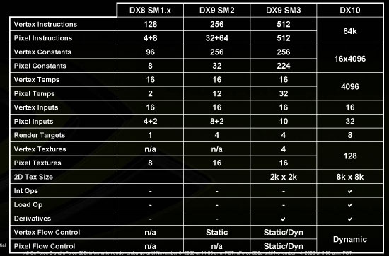
Along with these changes, Microsoft has made some lower level adjustments. Until now, shaders have been exclusively floating point. This means that operations like memory addressing and array indexing (which use integer values) must be done carefully if interpolation is to be avoided. With DX10, integer and bitwise operations have been added to the mix. This means programmers can make use of traditional data structures and memory operations. Increasing the flexibility of the hardware and enabling programmers to employ methods commonly used on more general purpose hardware will certainly be helpful in creating a better platform for developers to create the effects they desire.
Floating point operations have also been enhanced, as Microsoft has placed tighter requirements on how to handle the numbers. IEEE 754 is a specification that defines all aspects of floating point interaction. Sticking to such a standard allows programmers to guarantee that operations will be consistent between different types of hardware. Because Microsoft hasn't been as strict in the past, we've seen some issues where ATI and NVIDIA don't provide the exact same result due to rounding and accuracy differences. This time around, DX10 has very nearly IEEE 754 requirements. There are certain aspects of IEEE 754 that are not desirable in graphics hardware. These aspects have to do with over and underflow and denorms. The special results that are usually returned in these cases under IEEE specifications aren't as useful as clamping the value of a calculation to either the smallest possible result or largest possible result. With DX10, we do see the addition of NaN and infinity as possible results, and along with a better specification of accuracy and precision, those interested in general purpose computing on graphics processors (GPGPU) should be very happy.
What are Geometry Shaders?
A whole new shader type has been added this time around as well: Geometry shaders. These shaders are similar to vertex shaders in that they operate on geometry before it has been projected on to screen space where pixel processing can take over. Rather than operating on single vertices, however, geometry shaders operate on larger blocks: meshes. These meshes (made up of vertices) can be manipulated in a myriad of ways. Working with an object containing vertices gives programmer the ability to manipulate those vertices in relation to each other more easily. Vertices can even be added or removed from a mesh. The ability to write out data from the geometry shaders (rather than simply sending it on for pixel processing) will also allow software to reprocess vertices that have been added or altered by the geometry shaders. As an extension to geometry instancing, we will have more flexibility in manipulating instanced geometry in order to avoid the cut and paste look. All of these new features mean we should see things like particle systems move completely off of the CPU and on to the GPU, and geometry may begin to play a larger role in graphics in the future.
In the beginning, increasing the number of triangles that could be rendered in a scene was a huge factor in performance. After a certain point, software, CPUs, buses, and overhead in general started to get in the way of how much difference adding more triangles made. Rather than having millions of really tiny triangles moving around, it became much faster to use textures to simulate geometry. Currently, per pixel lighting combined with uncompressed normal maps do a great job of simulating a whole lot of geometry at the expense of a lot of pixel power. With the new 8k*8k texture sizes and other DX10 enhancements, there is a lot of potential for using pixel processing to simulate geometry even better. But the combination of unified shaders and geometry shaders in new hardware should start to give developers a whole lot more flexibility in how they approach the problem of fine detail in geometry.
G80: A Mile High Overview
Now that we know a little more about the requirements and direction of DX10, we can take a deeper look at where NVIDIA has decided to go with the architecture of G80. We will be seeing a completely new design based around a unified shader architecture. While DX10 doesn't require a unified architecture, it certainly does make a lot of sense to move in that direction.
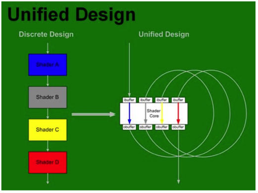
Inside G80, vertex, geometry, pixel shaders and more (more on this later) are all able to run on the same set of execution resources. In order to make this happen, the shader core needed to be made more general purpose and suitable for multiple usage scenarios. This is much like what we are used to seeing on a CPU, and as time moves on we expect these similarities to increase from both the CPU and GPU side. The design NVIDIA has come up, while very complex and powerful, is quite elegant. Here's a look at the block diagram for G80:
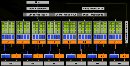
The architecture is able to use thread management hardware to dispatch different types of instructions on to the shader core. As vertices complete, their output can be used as input to geometry shaders back at the "top" of the shader core. Geometry shader output is then used as input to pixel shaders. Here's a quick conceptual representation of what we are talking about:
The sheer size of G80 is absolutely amazing; while NVIDIA wouldn't disclose exact die sizes let's look at the facts. The G80 chip is made up of 681 million transistors, more than a single core Itanium 2 or the recently launched Kentsfield, but manufactured on an almost old 90nm process. As a reference point, ATI's Radeon X1900 XTX based on the R580 GPU was built on a 90nm process yet it featured only 384 million transistors. NVIDIA's previous high-end GPU, the G71 based GeForce 7900 GTX was also built on a 90nm process but used only 278 million transistors. Any way you slice it, this is one huge chip. Architecting such a massive GPU has taken NVIDIA a great deal of time and money, four years and $475M to be exact. The previous record for time was almost 3 years at a lesser amount, but NVIDIA wouldn't tell us which GPU that was.
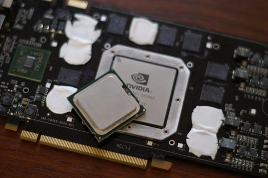
Intel's Quad Core Kentsfield on top, G80 on bottom
Despite very high clock speeds on the die and a ridiculous 681 million transistor count, power consumption of NVIDIA's G80 is quite reasonable given its target; on average, a G80 system uses about 8% more power than one outfitted with ATI's Radeon X1950 XTX.
You really start to get a sense of how much of a departure G80 is from previous architectures when you look at the shader core. Composed of 128 simple processors, called Stream Processors (SPs), the G80 shader core runs at a very high 1.35GHz on the highest end G80 SKU. We'll get into exactly what these stream processors are on the coming pages, but NVIDIA basically put together a wide array of very fast, specialized, but simple processors. In a sense, G80's shader core looks much like Cell's array of SPEs, but the SPs here are not nearly as independent as the SPEs in Cell.
Running at up to 1.35GHz, NVIDIA had to borrow a few pages from the books of Intel in order to get this done. The SPs are fairly deeply pipelined and as you'll soon see, are only able to operate on scalar values, thus through simplifying the processors and lengthening their pipelines NVIDIA was able to hit the G80's aggressive clock targets. There was one other CPU-like trick employed to make sure that G80 could have such a shader core, and that is the use of custom logic and layout.
The reason new CPU architectures take years to design while new GPU architectures can be cranked out in a matter of 12 months is because of how they're designed. GPUs are generally designed using a hardware description language (HDL), which is sort of a high level programming language that is used to translate code into a transistor layout that you can use to build your chip. At the other end of the spectrum are CPU designs which are largely done by hand, where design is handled at the transistor level rather than at a higher level like a HDL would.
Elements of GPUs have been designed at the transistor level in the past; things like memory interfaces, analog circuits, memories, register files and TMDS drivers were done by hand using custom transistor level design. But shaders and the rest of the pipeline was designed by writing high level HDL code and relying on automated layout.
You can probably guess where we're headed with this; the major difference between G80 and NVIDIA's previous GPUs is that NVIDIA designed the shader core at the transistor level. If you've heard the rumors of NVIDIA building more than just GPUs in the future, this is the first step, although NVIDIA was quick to point out that G80 won't be the norm. NVIDIA will continue to design using HDLs where it makes sense, and in critical areas where additional performance or power sensitive circuitry is needed, we'll see transistor level layout work done by NVIDIA's engineering. It's simply not feasible for NVIDIA's current engineering staff and product cycles to work with a GPU designed completely at the transistor level. That's not to say it won't happen in the future, and if NVIDIA does eventually get into the system on a chip business with its own general purpose CPU core, it will have to happen; but it's not happening anytime soon.
The additional custom logic and layout present in G80 helped extend the design cycle to a full four years and brought costs for the chip up to $475M. Prior to G80 the previous longest design cycle was approximately 2.5 - 3 years. Although G80 did take four years to design, much of that was due to the fact that G80 was a radical re-architecting of the graphics pipeline and that future GPUs derived from G80 will have an obviously shorter design cycle.
Digging deeper into the shader core
Many of the same patterns that lead designers of current hardware to their conclusions are still true today. For instance, pixels next to each other on the screen still tend to follow a very similar path through the hardware. This means that it still makes sense to process pixels in quads. As for changes, as hardware becomes more programmable, we are seeing a higher percentage of scalar data being used. In spite of the fact that much of the work done by graphics hardware is vector based, it becomes easier to schedule code if we are working with a bunch of parallel, independent, scalar processors. It is also more efficient to build separate units for texture addressing and filtering, and ATI has done this for quite some time now.
NVIDIA has finally decoupled the texture units from their shader hardware, enabling math and texturing to happen at the same time with no scheduling issues. They have also decided to implement their math hardware as a collection of scalar processors that can be used together to perform vector operations. NVIDIA calls the scalar processors Stream Processors (SPs), and they handle all the math performed in the shader core of G80.
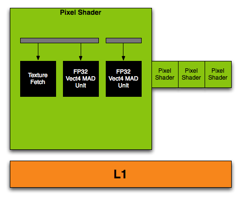
It isn't surprising to see that NVIDIA's implementation of a unified shader is based on taking a pixel shader quad pipeline, and breaking up the vector units into 4 scalar units. Now, rather than 4 pixel quads, we see 16 SPs per "quad" or block of stream processors. Each block of 16 SPs shares 4 texture address units, 8 texture filter units, and an L1 cache.
G70 Pixel Shader Quad
G80 Stream Processor Block
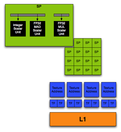
The fact that these SPs are now independent and scalar gives NVIDIA the ability to keep more of them busy more of the time. This is very important as programmers start to write longer more complex shaders. Even while working with vectors, programmers need to use scalar values all the time to manipulate and evaluate data.
Each Stream Processor is able to complete one MAD and one MUL per clock cycle. While this is based on maximum throughput, we can reasonably expect to achieve this even though the hardware is pipelined. In spite of the 4 or 5 cycles (depending on precision) latency of a MUL in Conroe, SSE is now capable of one MUL per cycle throughput (as long as there are no stalls in the pipeline). Latency of operations in G80 could be even longer and sustain high throughput, as most of the time we are working with code that isn't riddled with dependencies.
The fact that each SP is capable of IEEE 754 single precision and can sustain high throughput for MAD and MUL operations while running any type of shader code makes this hardware very powerful and more general purpose than ever.
As a thread exits the SP, G80 is capable of writing the output of the shader to memory. The fact that SPs can do this at any time (except after pixel shaders) goes beyond the DX10 spec of just allowing for stream output after the Geometry Shader. On previous hardware, data would have to go through every stage of the pipeline until a value was finally written out to the frame buffer. Now, we can write data out at the end of anything but a pixel shader (as pixel shaders must send their output straight over to the ROPs for processing). This will be a great benefit to GPGPU (general purpose computing on graphics processing units).
Branching
In order to talk generally about SPs and their capabilities, all the vertices, primitives, pixel components, etc. to be processed are referred to as threads. This way we can look at each SP as handling its own thread no matter what type of data is being processed. G80 is able to sustain "thousands" of threads at a time, but the actual number of threads that can be active at any given time is not disclosed. While all SPs can handle any type of thread, SPs that share resources must be running the same type of thread at any given time. In this way, each block of 16 SPs can be running one type of shader program on 16 threads. This indicates something about branch granularity as well. For vertex shaders, branch granularity is 16 vertices. For pixel shaders, branch granularity is 32 pixels (arranged in pairs of blocks of 4x4 pixels).
Branch granularity defines how many threads must follow the same path through data. When a group of 32 pixel threads all take the same branch, we don't have a problem. If even one thread must take a path that is different from the others, all 32 threads must be evaluated with both paths following the branch. The branch then defines what result each individual thread will keep and which it will discard. It's easy to see that optimum granularity is 1 thread, as no unnecessary work would be done. The way resources are allocated and the way instructions are run on SPs grouped together currently doesn't allow any more fine-grained branching. Here's a chart that address branch granularity:
| GPU | Branch Granularity |
| NVIDIA NV4x | ~1K pixels |
| NVIDIA G70 | ~256 pixels |
| ATI R580 | 48 pixels |
| NVIDIA G80 | 16 vertex 32 pixels |
Clearly G80 has the advantage here, as it's less likely that smaller groups of pixels will take different directions through a branch. This gives programmers the ability to more easily integrate branching into their code without getting a massive performance hit. If programmers are able to incorporate more branches, shader code can become more general purpose and we will see many more effects make their way into games. Now that G80 has caught up to ATI in terms of potential branch performance, we hope developers will take the reality of more complex code seriously.
Early-Z, Memory Interface
NVIDIA has added hardware for Early-Z to G80, after their current Z-Cull hardware which removes regions of pixels completely occluded by other geometry. Early-Z is a more fine-grained occlusion culling method that looks at a calculated Z value of a fragment before it hits the pixel pipeline. Z-Cull doesn't look at per fragment Z values, but uses a Z value based on geometry. While Z-Cull can get rid of large blocks of data it has issues handling surfaces that are only partially occluded or intersecting surfaces. Looking at individual depth values per pixel can help remove unnecessary fragments from heading down the pipeline only to be thrown out when the ROPs get to them.
The memory interface has been dramatically redesigned to support the access patterns of all of G80's independent stream processors. Given the theme of increasing granularity within G80 it's no surprise that we are now seeing 5 and 6 channels of GDDR rather than the 2 or 4 channels we have been used to for the past few years. 8800 GTX will have a 384 bit bus (6 x 64-bit channels), while the 8800 GTS will have a 320 bit wide connection to DRAM (5 x 64-bit channels). We would love to delve further into the details of G80's new memory interface, but NVIDIA isn't discussing the details of this aspect of their hardware.
General Purpose Processing
With all the talk about how general purpose G80 is, can we expect it to replace our shiny new quad core desktop processor? This isn't quite possible at this point due to the way most general purpose code uses the CPU. Many dependencies and low parallelism prevent NVIDIA from simply dropping this in a motherboard and running Windows on it.
But there are general purpose tasks that lend themselves well to the parallelism of G80, and NVIDIA is enabling developers to take advantage of this via a technology they call CUDA (Compute Unified Device Architecture).
The major thing to take away from this is that NVIDIA will have a C compiler that is able to generate code targeted at their architecture. We aren't talking about some OpenGL code manipulated to use graphics hardware for math. This will be C code written like a developer would write C.
A programmer will be able to treat G80 like a hugely parallel data processing engine. Applications that require massively parallel compute power will see huge speed up when running on G80 as compared to the CPU. This includes financial analysis, matrix manipulation, physics processing, and all manner of scientific computations.
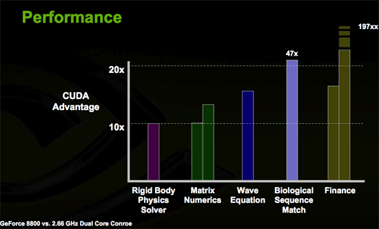
NVIDIA has written a totally separate driver for G80 that will be used to run compiled C code targeted at G80. The reason they've done this is because the usage model for GPGPU programming is so different from that of graphics. Both the graphics driver and the CUDA driver can be running on G80 at the same time. This may allow programmers to take advantage of CUDA for in game physics on a single card. The driver changes the conceptual layout of the GPU into something that looks more like this:
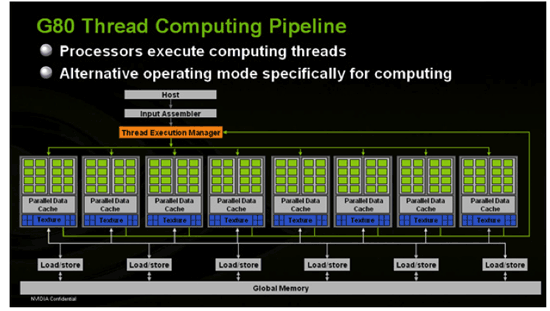
This design, along with stream output capabilities, allows programmers to treat the GPU like a general purpose data processing engine. Each block of 16 SPs is able to share data with each other and can perform multiple passes on the data without having to write out and read back in from the onboard graphics memory. Developers are given the ability to manage the caches themselves.
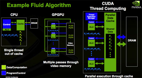
Will NVIDIA make an x86 CPU? Most likely not, but we may see NVIDIA produce even more general purpose CPUs for the handheld, CE, integrated markets. NVIDIA may end up becoming a producer of system on a chip solutions utilizing its graphics technology and simply expanding G80 to be more general purpose (and obviously get rid of some of the SPs in order to lower costs).
What is CSAA?
Taking another step forward in antialiasing quality and performance, NVIDIA is introducing Coverage Sample Antialiasing with G80. Coverage Sample AA is an evolutionary step forward in AA technology designed to improve how accurately the hardware is able to determine the area of a pixel covered by any given surface. CSAA can be thought of as extending MSAA. NVIDIA is calling all of their AA modes CSAA, even though common AA modes (2x, 4x, and now 8x (8xQ to NVIDIA)) are performed exactly the same way MSAA would be performed.
To enable modes that more accurately represent each polygon's coverage of a pixel, NVIDIA has introduced an "Enhance the application" option in their driver. This option will allow you to enable a desired MSAA mode in a game (either 4x or 8x) and then "enhance" it by enabling 8x, 16x, or 16xQ CSAA. This will make the 4xAA requested in the game look like 8xAA or 16xAA. Enhancing 8x to 16xQ gives the effect of 16xMSAA without the huge performance impact that would be associated with such a setting.
To understand how it comes together, lets take a quick look at fragments and the evolution of AA.
We usually refer to fragments as pixels for simplicity sake (and because Microsoft decided to use the term pixel shader rather than fragment shader in DirectX), but it helps to understand what the difference between a pixel and a fragment is when talking about AA methods. A pixel is simply a colored dot on the screen (or stored in a frame buffer). The different pieces of data that go into determining the color of a particular pixel are called fragments. For example, if 2 triangles cover the area of a single pixel, both will be processed as fragments. Texture look ups will be done for each at the pixel center, and a color and depth will be determined, and any of this data can be manipulated by a fragment (pixel) shader. Without AA (and ignoring blending, transparency, etc...), only the fragment that is nearest the viewer and covers the pixel center will determine the color of the pixel. Antialiasing techniques are used to make the final pixel color reflect an accurate blend of the colors that cover a pixel.
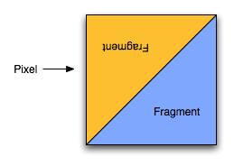
A sub-pixel can be thought of as a zoomed in look at the area a pixel covers, so for example instead of a single pixel it can be viewed as a 10x10 grid of sub-pixels. Current popular FSAA (full screen AA) methods use the calculated colors of multiple sub-pixels that fall within the area of a pixel rather than just the pixel center to determine the final color. Super Sample AA takes each of these sub-pixels through the entire pipeline to determine texture and pixel shader output at each location. This is very accurate, but wastes lots of processing power without providing a proportional benefit. This is because sub-pixels that fall on the same surface don't usually end up with very different colors. MSAA only looks at one textured/shaded sample point per fragment. The colors of the sub-pixels on a polygon are the same as the color at the center of the pixel, but each sub-pixel gets its own depth value. When two polygons cover the same pixel, we can end up with different colored sub-pixels. Blending these colors proportionally results in properly antialiased polygon edges.
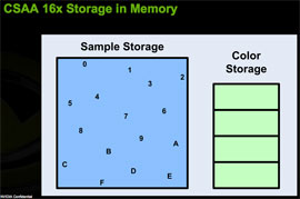
CSAA extends MSAA by decoupling color and depth values from the positions of the sample points within a pixel. Color values are determined at the pixel center, and color and depth data are stored in a buffer. The extension of this in CSAA comes in that we can look at more sample points in the pixel than we store color/Z data for. Under NVIDIA's 16x CSAA, four color values are stored, but the fragment coverage information for each of 16 sample points is retained. These coverage sample points are able to reference the appropriate color/Z data stored for the polygon that covers them.
 |
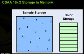 |
While NVIDIA couldn't go into much detail on the technology behind CSAA, we can extrapolate what's going on behind the scenes in order to make this happen. For each triangle that covers a pixel, each CSAA sample point gets a boolean value that indicates whether or not it is covered by the triangle. Color/Z data for the fragment are stored in a buffer for that pixel. For this whole thing to work, each CSAA sample point must also know what color in the buffer to indicate. If we assume position is predefined, the most storage that would be needed for each CSAA point is 4 bits (one boolean coverage value plus 3bits to index 8 color/Z values). The color and Z data will be significantly larger than 8 bytes per pixel, especially for floating point color data, so the memory footprint shouldn't be much larger than MSAA.
As fragments are sent out of the pixel shader, sub-pixel data is updated based on depth tests, and coverage samples and color/Z data will be updated as necessary. When the scene is ready to be drawn, the coverage sample points and color/Z data will be used to determine the color of a pixel based on each fragment that influenced it.
So what are the downsides? We have less depth information inside the pixel, but in most cases this isn't as important as color information. We do need to know depth at different sub-pixel positions in order to handle intersecting polygons, but doing this with a different level of detail than color information shouldn't have a big impact on quality.
The other drawback is that algorithms that require stencil/Z data at sub-pixel locations will not work correctly with CSAA in modes where there are more coverage samples than colors stored. In these cases, like with the stencil shadows used in FEAR, only the coverage samples located where color values are taken are used. This effectively reverts these algorithms to MSAA quality levels. CSAA will still be applied to polygon edges, and stencil algorithms will still work with the decreased level of antialiasing applied.
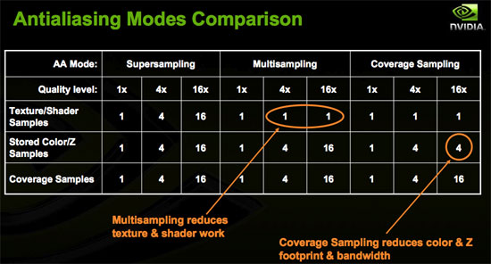
At a basic level, CSAA can provide more accurate coverage information for a pixel without the storage requirements of MSAA. This not only gives gamers an option to enable higher quality AA, but the option to enable higher quality AA without a large performance impact. While the explanation of how it does this may be overly complex, here's a simple table to help convey what's going on:
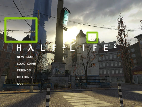
All of our image quality comparisons are 200 - 400% zooms on the two highlighted areas of the following image:
What really matters are image quality and performance. Does CSAA provide equivalent or better image quality to MSAA methods? We take a look at Half-Life 2 to find out. First up, we compare CSAA and MSAA in modes where only 4 color/z values are stored.

8X 8XQ
Hold mouse over links to see Image Quality
Here we can see that NVIDIA's 8x and 8xQ modes provide similar quality. The higher number of multisamples employed by 8xQ does seem to have a positive impact on thin line antialiasing, as seen with the antenna. Edges look about the same though.
Our DX9FSAAViewer won't show us the exact sample patterns for CSAA, but we can take a look at where ATI and NVIDIA are getting their color sample points:
| ATI |  |
 |
 |
| G70 |  |
 |
 |
| G80 |  |
 |
 |
| G80* |  |
 |
 |
*Gamma AA disabled
As we can see, NVIDIA's 8x color sample AA modes use a much better pseudo random sample pattern rather than a combination of two rotated grid 4xAA patterns as in G70's 8xSAA.
While it is interesting to talk about the internal differences between MSAA and CSAA, the real test is pitting NVIDIA's new highest quality mode against ATI's highest quality.

G70 4X G80 16XQ ATI 6X
Hold mouse over links to see Image Quality
Stacking up the best shows the power of NVIDIA's CSAA with 16 sample points and 8 color/z values looking much smoother than ATI's 6xAA. Compared to G70, both ATI and G80 look much better. Now let's take a look at the performance impact of CSAA. This graph may require a little explanation to understand, but it is quite interesting and worth looking at.
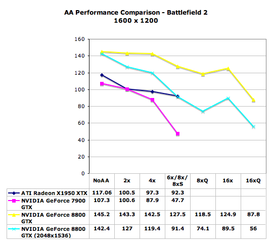
As we move from lower to higher quality AA modes, performance generally goes down. The exception is with G80's 16x mode. Its performance is only slightly lower than 8x. This is due to the fact that both modes use 4 color samples alongside more coverage samples. We can see the performance impact of having more coverage samples than color samples by looking at the performance drop from 4x to 8x on G80. There is another slight drop in performance when increasing the number of coverage samples from 8x to 16x, but it is almost nil. With the higher number of multisamples in 8xQ, algorithms that require z/stencil data per sub-pixel may look better, but 16x definitely does great job with the common edge case with much less performance impact. Enabling 16xQ shows us the performance impact of enabling more coverage samples with 8x multisamples.
It is conceivable that a CSAA mode using 32 sample points and 8 color points could be enabled to further improve coverage data at nearly the same performance impact of 16xQ (similar to the performance difference we see with 8x and 16x). Whatever the reason this wasn't done in G80, the potential is there for future revisions of the hardware to offer a 32x mode with the performance impact of 8x. Whether the quality improvement is there or not is another issue entirely.
What's Gamma Correct AA?
Gamma correction is a technique used to map linearly increasing brightness data to a display device in a way that conveys linearly increasing intensity. As displays are nonlinear devices, gamma correction requires a nonlinear adjustment to be made to brightness values before being sent to the display. Ideally, gamma corrected linear steps in the brightness of a pixel will result in linear steps in perceived intensity. The application in antialiasing is that high contrast edges can appear under aliased if the brightness of a pixel isn't adjusted high enough for humans to perceive an increase in intensity after being displayed by the monitor.
Unfortunately, gamma correcting AA isn't always desirable. Different CRT, LCD, and TVs have different gamma characteristics that make choosing one gamma correction scheme more or less effective per device. It can also result in brighter colored sub-samples having a heavier influence on the color of a pixel than darker sub-samples. This causes problems for thing like thin lines.
To illustrate the difference, we'll look at images of Half-Life taken on G80 with and without gamma correction enabled.

G80 4X Gamma ATI 4X Gamma
Hold mouse over links to see Image Quality
At 4xAA with gamma correction enabled, it looks like ATI is able to produce a better quality image. Some of the wires and antenna on NVIDIA hardware area a little more ragged looking while ATI's images are smoothed better.
What's Transparency AA?
Transparency AA is NVIDIA's method of applying AA to transparent textures. Because MSAA only looks at one texture sample per pixel per polygon where more than one polygon slices a pixel area, it is not able to smooth jagged edges in transparent textures. In order to combat this, NVIDIA applies supersample AA to transparent textures. Their multisample transparency AA really doesn't do much for visual quality, so we will be ignoring it today. It only allows multisample through transparent texture areas and not of the texture itself.
Supersample AA performs a texture lookup at each sub-pixel to determine how much of the pixel falls on a transparent area of the texture and how much falls on an opaque area. The analog in ATI hardware is called Adaptive AA, which does basically the same thing. This generally has a very large performance impact for 3D scenes with many transparent textures (fence, bushes, leaves, and the like).
All screenshots on this page are 400% zooms of the highlighted portion of the following Half Life 2 screenshot:
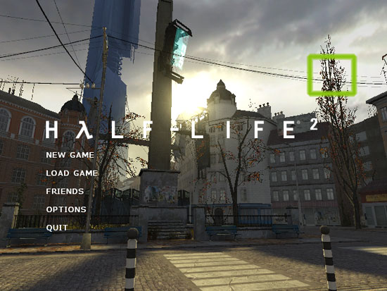
Here's a look at Half-Life 2 with and without Transparency AA. We can clearly see how the leaves of the trees get smoothed out and look much better.

G70 4X No Gamma G80 4X No Gamma ATI 4X Gamma
Hold mouse over links to see Image Quality
G70 and G80 don't look that different, but the R580 creates a kind of mushy look around the trees. This is another side effect of gamma correct AA and its potential negative impact on image quality. Worse examples include wire mesh or fences built with transparent textures: gamma correct AA can end up making parts of a fence disappear. Ideally, if we could apply gamma correct AA to high contrast edges and disable it for everything else, we'd see an image quality improvement. But the downsides just keep piling up with thin lines and transparent textures causing problems for gamma correction.
While transparency AA does enhance image quality a good deal, we do need to consider the performance impact. We'll revisit our antialiasing scaling graph from our CSAA page with Transparency and Adaptive AA enabled.
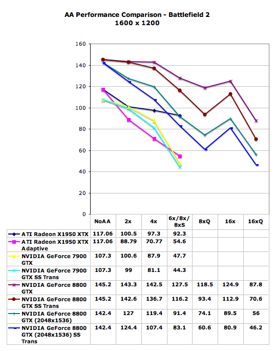
With G80, we see great performance at high resolution with high levels of AA while Transparency AA is enabled. With this level of performance, as long as R600 is able to keep up, we would love to check the Transparency AA check box every time we test with AA. For now, the performance degradation in R580 is just too high to justify at resolutions over 1600x1200 in most cases. An increase in resolution to a comparable performance level will net a higher gain in image quality.
Texture Filtering Image Quality
Texture filtering is always a hot topic when a new GPU is introduced. For the past few years, every new architecture has had a new take on where and how to optimize texture filtering. The community is also very polarized and people can get really fired up about how this company or that is performing an optimization that degrades the user's experience.
The problem is that all 3D graphics is an optimization problem. If GPUs were built to render every detail of every of every scene without any optimization, rather than frames per second, we would be looking at seconds per frame. Despite this, looking at the highest quality texture filtering available is a great place from which to start working our way down to what most people will use.
The good news is that G80 completely eliminates angle dependent anisotropic filtering. Finally we have a return to GeForce FX quality anisotropic filtering. When stacked up against R580 High Quality AF with no optimizations enabled on either side (High Quality mode for NVIDIA, Catalyst AI Disabled for ATI), G80 definitely shines. We can see at 8xAF (left) under NVIDIA's new architecture is able to more accurately filter textures based on distance from and angle to the viewer. On the right, we see ATI's angle independent 16xAF degrade in quality to a point where different texture stages start bleeding into one another in undesirable ways.

G80 Normal Quality AF G80 High Quality AF
Hold mouse over links to see Image Quality
The thing to remember is that, even when all optimizations are disabled, there are other optimizations going on that we can't touch. There always will be. The better these optimizations get, the faster we will be able to render accurate images. Gaining more control over what happens in the hardware is a nice bonus, but disabling optimization for no reason just doesn't make sense. Thus, our tests will be done at default texture filtering quality on NVIDIA hardware. In order to understand the performance impact of High Quality vs. Quality texture filtering on NVIDIA hardware, we ran a few benchmarks with as many optimizations disabled as possible and compared the result to our default quality tests. Here's what we get:
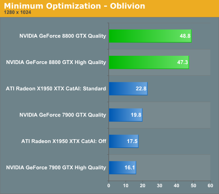
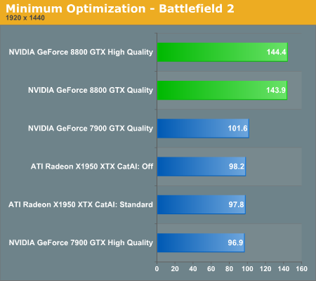
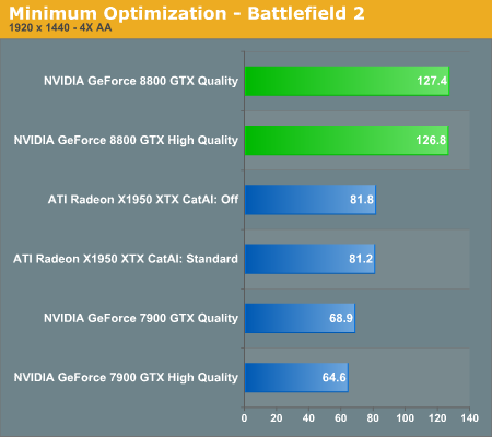
We can clearly see that G70 takes a performance hit from enabling high quality mode, but that G80 is able to take it in stride. While we don't have the ability to specifically disable or enable optimizations in ATI hardware, Catalyst AI is the feature that dictates how much liberty ATI is able to take with a game, from filtering optimizations all the way to shader replacement. We can't tell if the difference we see in Oblivion is due to shader replacement, filtering, or some other optimization under R580.
Image Quality: Summing it All Up
With NVIDIA's new method of acquiring a more detailed blur via CSAA, angle independent anisotropic filtering, and high performance with Transparency AA, potential image quality is improved over G70 and R580. The new architecture is capable of floating point frame buffer blends and antialiasing of floating point data. ATI has continually called this ability HDR+AA, and while it is better to be able to use full floating point for HDR, this isn't the only solution to the problem. There are some rendering techniques that employ MRTs (Multiple Render Targets) that will still not allow AA to be performed on them alongside HDR. There are also HDR techniques that allow antialiasing to be performed along with HDR without the need for AA + floating point (like games based on Valve's Source engine).
In any case, we've already covered the major differences in AA and AF modes and we even looked at how the optimizations affect image quality. For this section, we'll take a look at three different cases in which we employ the non-AA graphics settings we will be using in our performance tests. We are looking for differences in alpha blending, effective AF level in a game, and shader rendering. We didn't see anything that stood out, but feel free to take a look for yourselves.
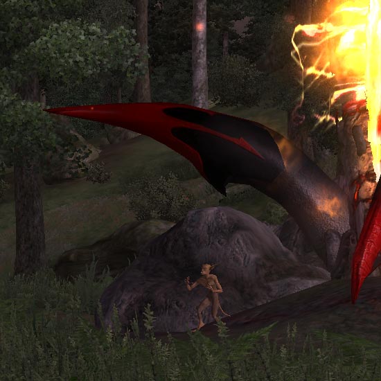
G70 G80 ATI
Hold mouse over links to see Image Quality
The 8800 GTX and GTS
Today we expect to see availability of two cards based on NVIDIA's G80 GPU: the GeForce 8800 GTX and 8800 GTS. Priced at $599 and $449 respectively, the two cards, as usual, differ in clock speeds and processing power.
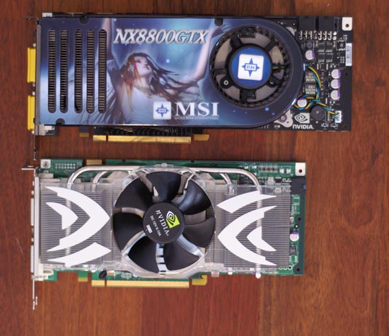
8800 GTX (top) vs. 7900 GTX (bottom)
The 8800 GTX gets the full G80 implementation of 128 stream processors and 64 texture fetch units. The stream processors are clocked at 1.35GHz with the rest of the GPU running at 575MHz. The GTX has six 64-bit memory controllers operating in tandem, connected to 768MB of GDDR3 memory running at 900MHz. GDDR4 is supported but will be introduced on a later card.
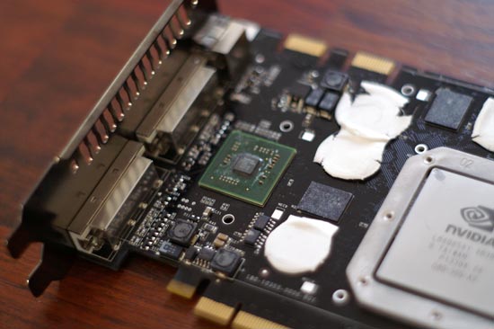
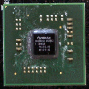
NVIO: Driving a pair of TMDS transmitters near you
You get two dual-link DVI ports driven by NVIDIA's new NVIO chip that handles TMDS and other currently unknown functions. Keeping a TMDS on-die is a very difficult thing to do, especially if you have logic operating at such high clock speeds within the GPU, so with G80 NVIDIA had to move the TMDS off-die and onto this separate chip. The NVIO chip also supports HDCP, but you do need the crypto ROM keys in order to have full HDCP support on the card. That final decision is up to the individual card manufacturers, although at this price point we hope they all choose to include HDCP support.
The 8800 GTX has two PCIe power connectors and two SLI connectors:
![]()
Two SLI connectors on the 8800 GTX
![]()
Bridges in action
The dual power connectors are necessary to avoid drawing more power from a single connector than the current ATX specification allows for. The dual SLI connectors are for future applications, such as daisy chaining three G80 based GPUs, much like ATI's latest CrossFire offerings.
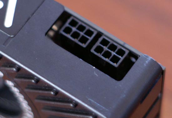
dual power connectors
The GeForce 8800 GTS loses 32 SPs bringing it down to 96 stream processors and 48 texture fetch units. The shader core runs at 1.2GHz, while the rest of the GTS runs at 500MHz. The GTS also has only five 64-bit memory controllers with 640MB of GDDR3 memory running at 800MHz.
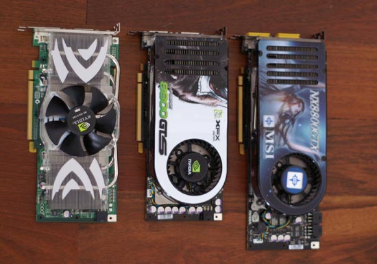
7900 GTX (left) 8800 GTS (middle) 8800 GTX (right)
The 8800 GTS has the same NVIO chip as the 8800 GTX, but the board itself is a bit shorter and it only features one SLI connector and one PCIe power connector.
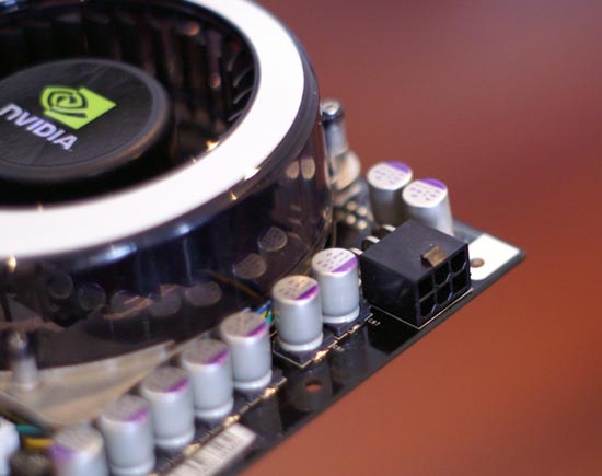
Only one power connector on an 8800 GTS
![]()
...and only one SLI connector
Both cards are extremely quiet during operation and are audibly indiscernible from a 7900 GTX.
Power Supply Requirements
NVIDIA does recommend at least a 450W power supply that can deliver up to 30A on the +12V rail. For our testing we used OCZ's GameXStream 700W power supply, which features two PCIe power connectors, perfect for the 8800 series.
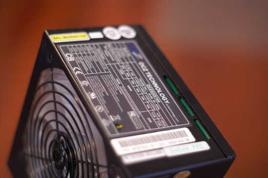
OCZ sent us a pre-release version of its 1kW power supply for use in our GeForce 8800 GTX SLI tests.
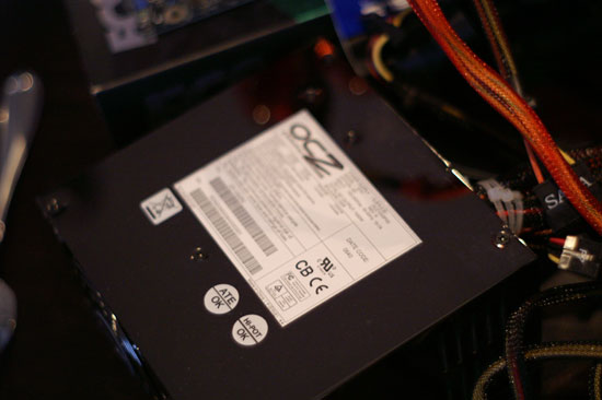
Armed with four PCIe power connectors, the 1kW unit handled the incredible load placed on it by two 8800 GTX cards without a problem. Total system power consumption when running our benchmarks, at times, peaked at over 520W with the SLI setup.
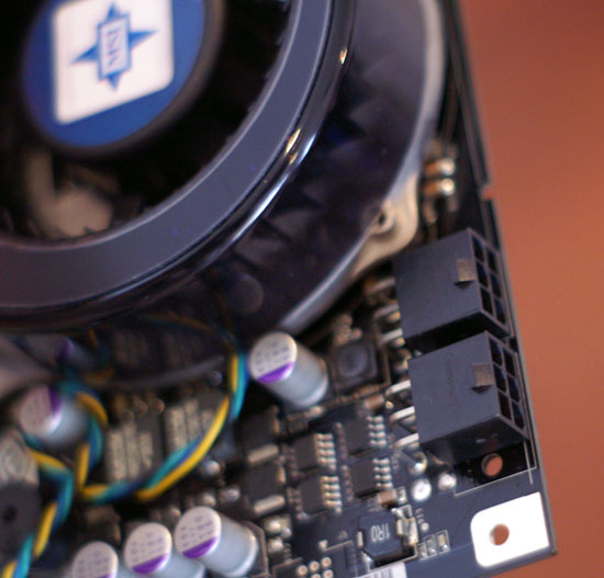
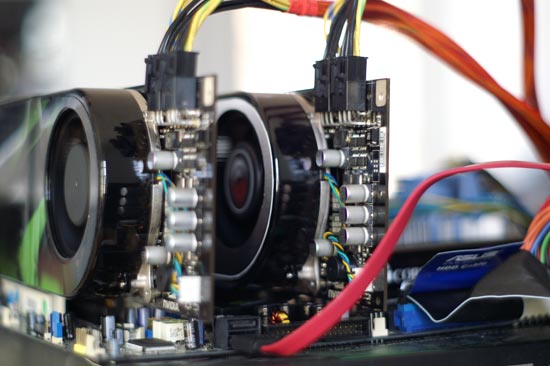
Two 8800 GTX cards in action; four power cables are necessary
The 680i Platform
Alongside the GeForce 8800 GTX and GTS, NVIDIA is launching a brand new chipset for Intel processors, the nForce 680i (and 650i SLI and Ultra). Our own Wesley Fink has published an in-depth look at the new chipset, but we felt the release significant enough to comment on some of its features here in this review.
For the most part, competing with Intel for its chipset business is an effort in futility. The companies that have tried have ended up either segregated to the low end of the market or kept to an extremely small niche. The past has proven that it is simply very difficult for a company that isn't Intel to produce a better performing chipset for Intel processors.
The multi-GPU era has changed things a bit, because now all of the sudden there's a new feature that Intel can't simply support on its chipsets. It took a while but ATI eventually allowed Intel to support CrossFire on its chipsets, but who knows how long that will last given ATI's new owner. While ATI caved in and supported Intel, NVIDIA would not capitulate. NVIDIA is like a mini-Intel and just like the big version, it doesn't play well with others. Licensing SLI for use on Intel chipsets was simply not in the cards; instead NVIDIA used SLI support as a reason for Intel users to consider NVIDIA chipsets. As NVIDIA continues to have the stronger multi-GPU lineup (although ATI has recently started fixing some of its problems with CrossFire), the SLI brand remains strong.
Although behaving like a veteran chipset manufacturer, NVIDIA is still a relative newcomer to the chipset business, but one thing we have seen from the boys in green is that they definitely learn from their mistakes. Dating back to the original nForce chipset, NVIDIA fell flat on its face with its first attempt at PC core logic, but bounced back to topple VIA with its nForce2 chipset. And it's that nForce to nForce2 transition that we're seeing here again with NVIDIA's nForce 680i SLI.
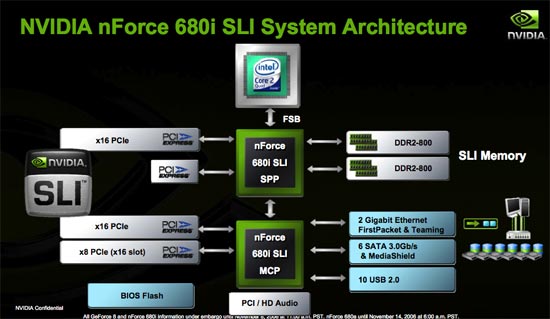
The 680i SLI is strictly a high end chipset, as the lower end of the market will still be serviced by NVIDIA's 570 SLI. The 680i supports all of the checkbox features: 1066MHz FSB (with unofficial support for higher speeds), dual channel DDR2-800, two PCIe x16 slots, one PCIe x8, 2 GbE ports, 6 SATA, 10 USB and HD Audio.
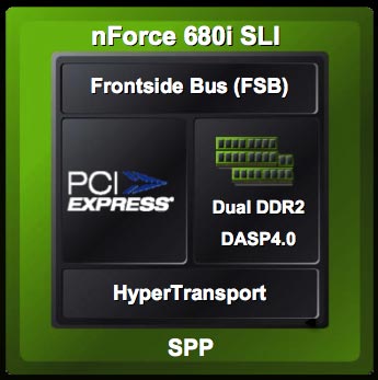
There are some pretty unique features about the new chipset. For starters it is the first NVIDIA core logic to be built on a 90nm process. The 680i SPP (aka North Bridge) is built on TSMC's 90nm process and thus ends up running cooler and can be overclocked more than NVIDIA's previous offerings in the area. The South Bridge (680i MCP) is still a 130nm chip but its functions are far less critical than those of the North Bridge.
In the 680i SPP is an updated version of NVIDIA's pre-fetching core called DASP. The major change to the 680i's DASP is that it is optimized for the memory access patterns of Conroe and Kentsfield which apparently are very different from NetBurst CPUs of the past. Given the aggressive prefetching done by the new Core processors and the large shared L2 cache, it isn't surprising to find out that memory controllers tuned to older Intel processors might not be best optimized for Core.
The primary function of the 680i's DASP is to examine memory access patterns and prefetch data into a local buffer that it thinks the processor will need at a later point in time. The updated version of DASP prefetches one cache line (64B) at a time into an internal buffer, although NVIDIA wouldn't disclose the size of the buffer.
We couldn't get much more information on DASP 4.0 from NVIDIA other than it supports prioritizing of reads over writes (to avoid read-to-write delays from random memory requests) and that a number of proprietary algorithms are used to make sure that prefetching doesn't occur when the CPU actually needs data from the memory controller.
Overclocking is a very large part of the new 680i chipset, and Wes' review of it goes into great detail about what exactly is possible with this new platform. For us, the other interesting part of the 680i platform is that, for the first time, NVIDIA is allowing its partners to sell NVIDIA engineered and designed 680i motherboards.
It has often been the case that a chipset maker's reference board has far more bells and whistles than anything its motherboard partners actually sell on the market. NVIDIA was growing weary of this being the case and instead effectively engineered a reference board that could be sold in retail.
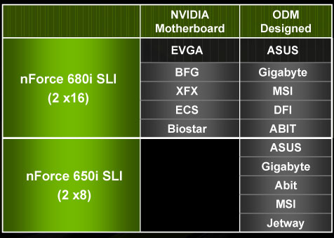
Motherboard makers can still choose to design their own 680i boards, but some have opted to simply rebrand NVIDIA's design.
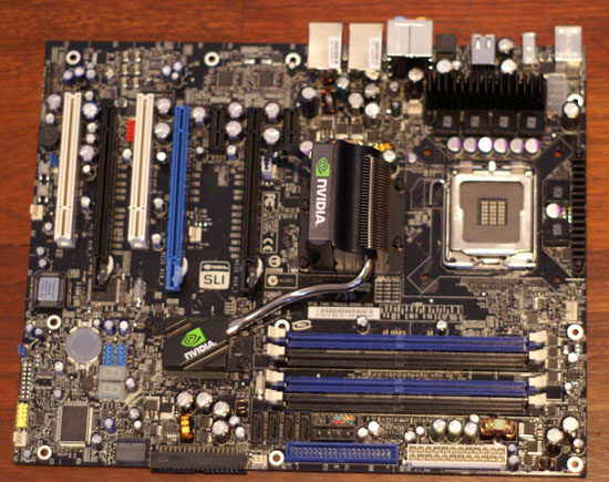
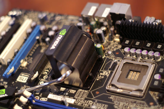
We ran all of our tests for this review on NVIDIA's nForce 680i SLI motherboard; this particular one is branded by EVGA. We were extremely pleased with the stability, BIOS, attention to detail and overall performance of the 680i solution. The decision to introduce NVIDIA designed 680i boards also shows how far NVIDIA has come as a manufacturer; if you want something done right, you sometimes have to do it yourself, and that's exactly what NVIDIA decided to do here. Honestly, the only downside is its estimated cost of $229.
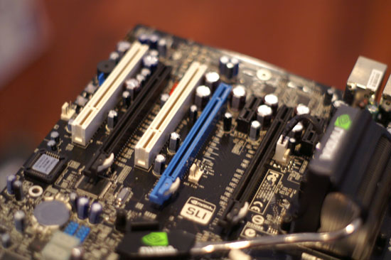
Three PCIe x16 slots (one is an x8 electrical)
NVIDIA is also introducing a lower cost 650i SLI chipset with only two x8 PCIe slots, but there will be no NVIDIA engineered boards available based on that chipset.
The Test
In our game tests, in every game we enabled the highest level of quality possible as far as features and effects are concerned. Where it was an option we enabled 16xAF in game. In games with "texture filtering" settings (like Battlefield 2) we endabled the highest level of filtering in game. In Oblivion we forced 16xAF in the control panel.
With the exception of Oblivion, we enabled AA in all our general performance tests. Where we were given the option, we chose 4xAA. In Black & White 2 and Company of Heroes we enabled AA in game (High for BW2 and Enabled for CoH).
| CPU: | Intel Core 2 Extreme X6800 (2.93GHz/4MB) |
| Motherboard: |
EVGA nForce 680i SLI Intel BadAxe |
| Chipset: | NVIDIA nForce 680i SLI Intel 975X |
| Chipset Drivers: |
Intel 7.2.2.1007 (Intel) NVIDIA nForce 9.35 |
| Hard Disk: | Seagate 7200.7 160GB SATA |
| Memory: | Corsair XMS2 DDR2-800 4-4-4-12 (1GB x 2) |
| Video Card: | Various |
| Video Drivers: |
ATI Catalyst 6.10 NVIDIA ForceWare 96.97 NVIDIA ForceWare 91.47 (G70 SLI) |
| Desktop Resolution: | 2560 x 1600 - 32-bit @ 60Hz |
| OS: | Windows XP Professional SP2 |
A Few Words about Performance Per Watt
In the coming performance pages we will be looking at the performance of the 8800 series of graphics cards as well as power consumption and performance per watt of our test systems. Note that the power consumption and performance per watt we are reporting is for the entire system, and not just the GPU, so while you don't get an idea of the performance per watt of the GPU alone, you do get an idea of the performance per watt of the entire system configured as we have. This is an important distinction to keep in mind as performance per watt of the GPU alone could be very different than what we're reporting here. What these numbers will tell you however is the most power efficient setup we have configured here today.
We're going to dispense with a lot of the introductory commentary for all of our gaming benchmarks, as we already have a ton of material to present. At this point, most of you are already familiar with what benchmarks we use and how they are run. If not, you should easily be able to find the information in a previous article. So, rather than adding hundreds of words of repeat text, we're just going to cut straight to the chase and talk about performance.
Company of Heroes Performance
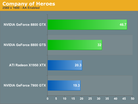
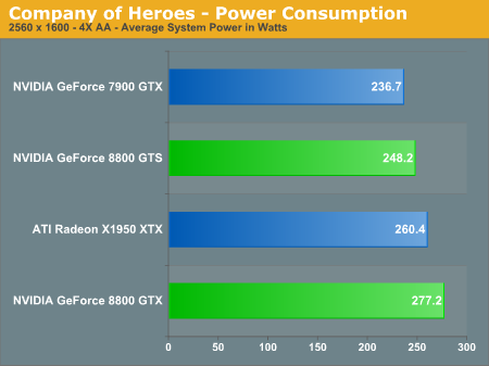
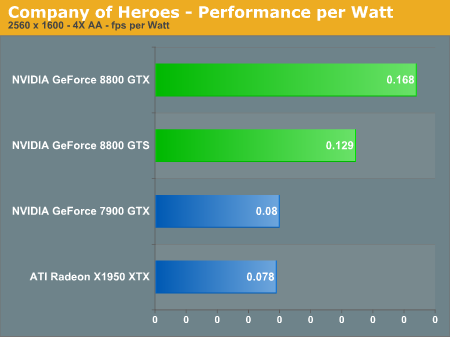
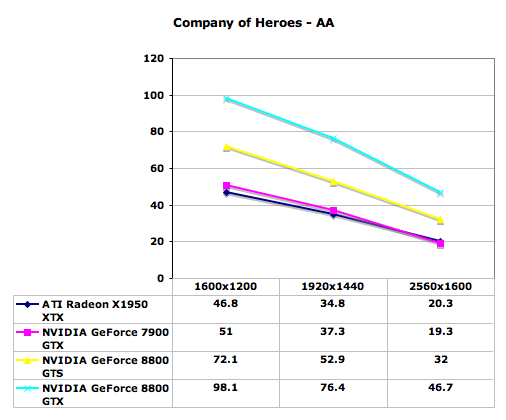
Starting with Company of Heroes, we have a game that really stresses the graphics card at higher settings, though in the past we've also shown that it tends to be CPU limited with different detail settings. Running maximum details, all of the cards still managed to deliver acceptable gameplay at 1600x1200 or lower resolutions. 1920x1440 is still playable as well, but if you have a 30 inch LCD running 2560x1600 and you want to run with antialiasing, you're really going to need a GeForce 8800 series card. The GeForce 8800 is clearly more powerful than anything ATI currently offers, which is to be expected as it's a next-generation card competing with current generation hardware. What's impressive is that the 8800 GTX is basically as fast running 2560x1600 as the GeForce 7900 GTX or Radeon X1950 XTX running at 1600x1200. Put another way, a single 8800 GTX is over twice as fast as a single X1950 XTX in all of the tested resolutions, and it's also about twice as fast as a 7900 GTX.
As far as multiple graphics card configurations go, Company of Heroes currently did not show any performance improvements. Most likely that means that NVIDIA and ATI drivers have not been properly optimized for this game at present. This is a problem that occurs periodically with new titles, and it's always frustrating to get a new game only to find out that it isn't properly using your hardware -- especially if you've shelled out the money for dual graphics cards. This is why we have repeatedly recommended in the past that you purchase a faster single graphics card rather than moving to dual GPUs, up to the point where you basically have the fastest single graphics card available. GeForce 8800 GTX now holds the title of fastest single GPU, so if you were previously looking to spend $800 on a couple of GPUs, you should seriously consider a single 8800 GTX instead. The DirectX 10 support is merely icing on the cake.
F.E.A.R. Performance
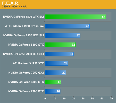
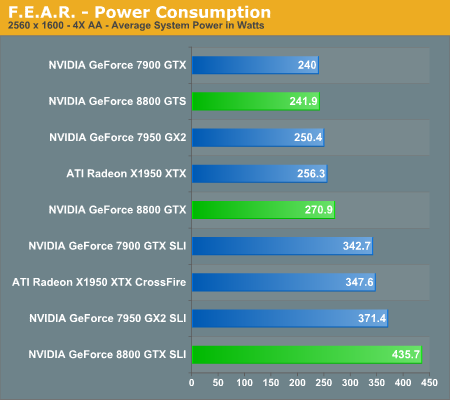
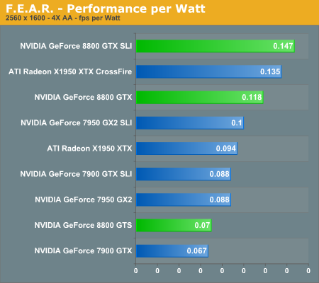
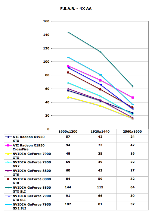
With the latest 1.08 patch, F.E.A.R. has gained multi-core support, potentially using even up to quad core CPUs in order to deliver improved performance. We were able to confirm a performance increase with Core 2 Duo, and we will try to take a look at whether or not Core 2 Quad helps in the near future. Either way, this means that we should now be completely GPU limited in F.E.A.R. testing.
The new GeForce 8800 GTX card still manages to come out faster than the competition, but this time a single 8800 GTX is not able to surpass the performance of dual X1950 XTX cards (or 7900 GTX SLI for that matter). Quad SLI also manages to make a decent showing in this particular benchmark, coming in second place except at the highest resolution. Meanwhile, GeForce 8800 GTS doesn't fare as well, only managing to tie the X1950 XTX for performance, and it even loses that battle at 2560x1600. F.E.A.R. is a game that can use a lot of memory bandwidth, so it's likely that the 2GHz GDDR4 memory on the X1950 XTX is helping out.
If money isn't a concern, 8800 GTX SLI will finally allow you to play F.E.A.R. at 2560x1600 with 4xAA without dropping below 30 FPS. Is that really necessary? Probably not to most people, but if a similar situation exists in other games it becomes a bit more feasible.
Black & White 2 Performance
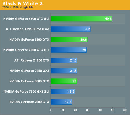
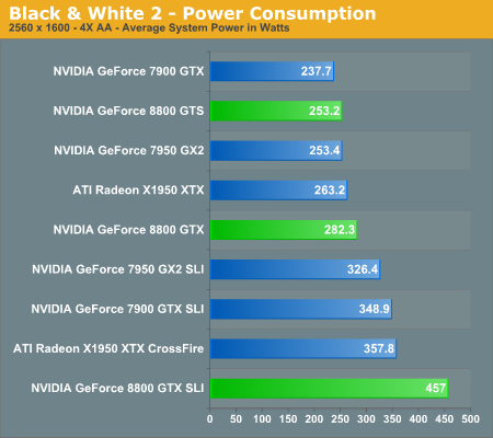
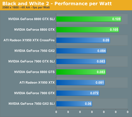
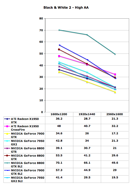
The GeForce 8800 GTX once again makes an impressive showing in Black and White 2, nearly equaling the performance of X1950 XTX CrossFire and GeForce 7900 GTX SLI in all tested resolutions. Even at these very high quality settings, 8800 GTX SLI becomes CPU limited below 1920x1440, so you will definitely want a large monitor before even considering two of these cards. Quad SLI has a pretty poor showing in this game, which is a problem that has plagued QSLI since it first became available. In games that can leverage the technology, it can improve performance quite a bit, but in other titles Quad SLI has difficulty even keeping up with 7900 GTX SLI.
GeForce 8800 GTS is quite a bit slower than its big brother, offering performance more or less equal to the X1950 XTX and the 7950 GX2. It still has the DirectX 10 advantage, but in current generation titles it's more a case of remaining competitive rather than adding a substantial performance increase. In this game, GeForce 8800 GTS is only ~15% faster than 7900 GTX. Two 8800 GTS cards in SLI should still take second place overall, but it's going to be a distant second.
Oblivion Performance
We aren't listing the table with all the settings we used because this time it's easy. We cranked everything up to the maximum setting. Every slider maxed and every feature enabled (with the exception of bloom and AA which are precluded by HDR). Taking into account just how stressful this game is under balanced quality settings, we can easily see just how incredible the 8800 GTX really is.
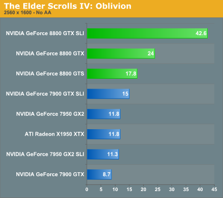
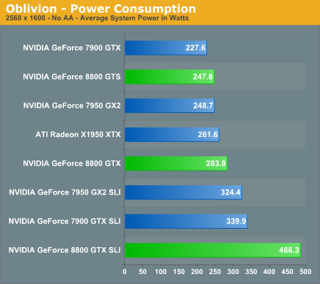
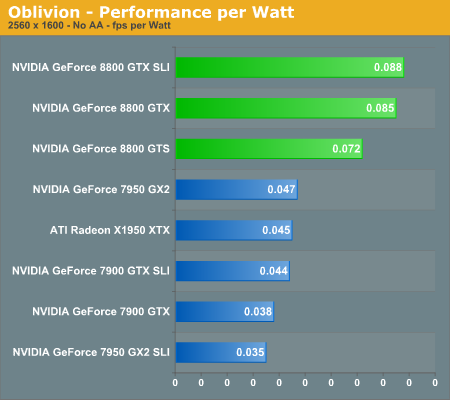
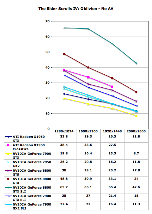
Oblivion has been one of the most demanding games in terms of graphics requirements ever since its launch. Up till now, ATI had a pretty substantial performance lead over almost anything NVIDIA could offer in this game, short of the 7950 GX2. With the launch of the GeForce 8800 series, the tables have turned, and quite dramatically. Not only does a single 8800 GTX card outperform any other current configuration (with the likely exception of 8800 GTS SLI, which we weren't able to test yet), but even the GeForce 8800 GTS is able to perform nearly as fast as X1950 XTX CrossFire, and slightly better than 7900 GTX SLI.
The 8800 GTX SLI is still the bottleneck in this game at resolutions above 1280x1024, showing just how demanding Oblivion is when it comes to graphics cards. ATI's CrossFire also scales better than NVIDIA's SLI in this title, gaining on average ~75% with CrossFire versus ~65% with SLI. Of course, we have to temper that statement by pointing out that X1950 CrossFire did not run properly at 2560x1600.
Battlefield 2 Performance
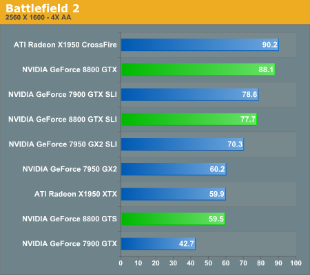
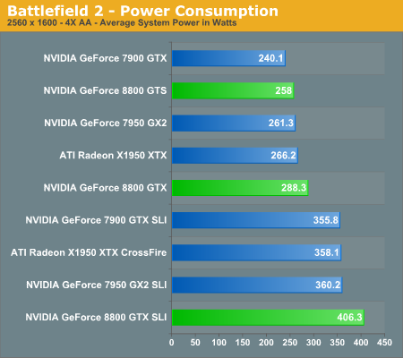
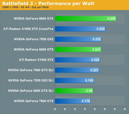
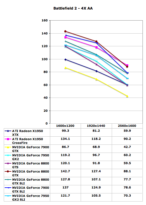
We had hoped to use Battlefield 2142 for testing, but the benchmarking utilities that came with 2142 are actually a step back relative to Battlefield 2. We would also like to get a benchmark using a Titan map, and there are difficulties with doing so (you need to be running the server in order to record a demo in multiplayer). For now, we return to Battlefield 2.
Despite the fact that Battlefield 2 has been available for quite some time, this is our first taste of a game that clearly has issues with 8800 GTX SLI. The single 8800 GTX card is able to place at the top of the performance charts, which is good news. The 8800 GTS comes in faster than the single ATI and GeForce 7900 cards, matching the performance of the 7950 GX2. Unfortunately, 8800 GTX SLI currently performs slower than 7900 GTX SLI and X1950 XTX CrossFire. We would expect updated drivers to fix this issue, though honestly just about every one of the tested graphics cards is capable of running at maximum resolution with 4xAA.
Prey Performance
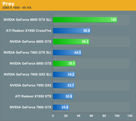
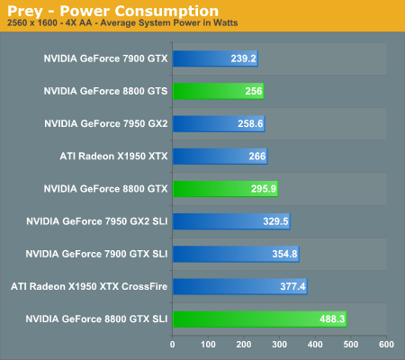
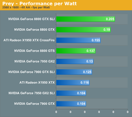
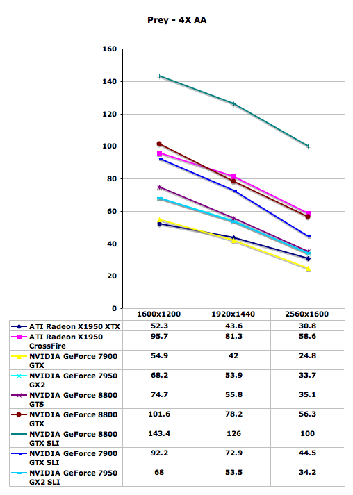
With Prey being based off of the Doom 3 engine, only with some enhancements, scores tend to be quite a bit lower than many other games. At our maximum detail settings, dual graphics cards were previously required to play at the highest resolution. Now, a single 8800 GTX card is once again able to equal the performance of X1950 XTX CrossFire, which is no small achievement. The reduction in pixel and vertex processing power results in the 8800 GTS performing quite a bit lower, although it still manages to outperform 7950 GX2 by a small margin.
Quad SLI continues to be a disappointing prospect, providing no performance increase over a single GX2 card. The release of GeForce 8800 pretty much seals the fate of Quad SLI as well, as it's doubtful that NVIDIA will continue to invest time in optimizing the QSLI drivers when they have new GPUs that could make better use of optimizations. We can only hope that most of you didn't get sucked in by the marketing.
Half Life 2: Episode One Performance
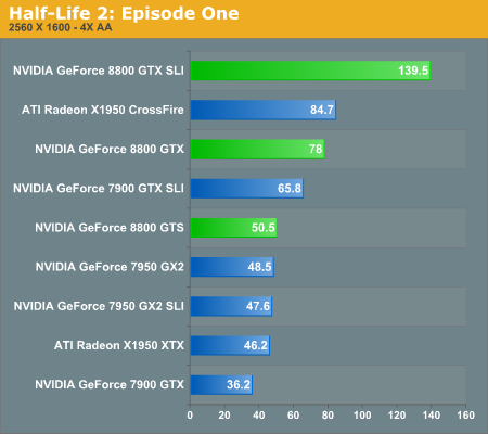
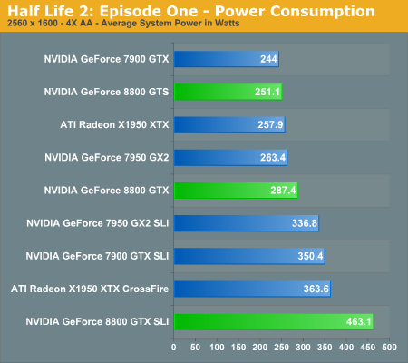
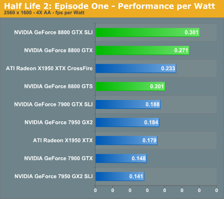
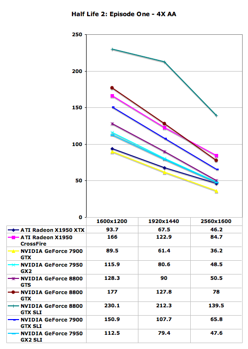
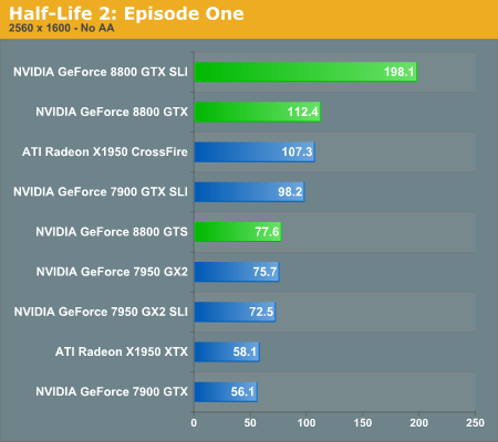
Having just visited Valve to discuss their multi-core and multithreading plans, it's interesting to consider their claims that they are more CPU limited than GPU limited. The only one of these high-end graphics configurations that isn't completely GPU limited at the tested resolutions is the 8800 GTX SLI setup, which is CPU limited to approximately 230 frames per second. Apparently, Valve intends to make a lot more use of your CPU in the near future, since we're still testing Source engine performance without multithreading support.
Besides the impressively expensive 8800 GTX SLI, even the slowest of the tested configurations is able to run at 2560x1600 4xAA with reasonable performance. A single 7900 GTX might be a bit choppy, although disabling antialiasing should cure that problem, but some levels and areas in Episode One should have lower overall frame rates than this particular demo script. In that case, the single 8800 GTX once again ties X1950 XTX CrossFire for second place, with 7900 GTX SLI trailing by 15%-20%. 8800 GTS comes next, outperforming all of the remaining single card offerings.
AA Disabled Performance
Up to this point, most of our benchmarks have been run with 4xAA, as we feel most people considering something like the new 8800 GTX are going to be interested in image quality as well as performance. If you don't care about antialiasing, the need for such fast graphics cards trails off quickly, as you'll see here.
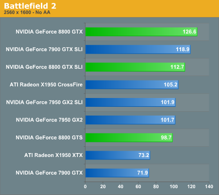
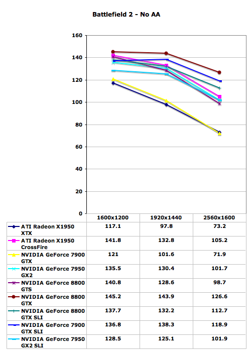
The 8800 GTX SLI still has issues with Battlefield 2, but more importantly you see the clustering of all of the high-end graphics configurations once antialiasing is disabled. Discounting the single ATI X1950 XTX and GeForce 7900 GTX cards, the spread among all the cards is about 20%-25%. Battlefield 2 is also clearly beginning to run into CPU limitations, with many of the cards showing very little in the way of performance drops when going from 1600x1200 to 1920x1440. When 8800 GTX SLI is fixed, we expect to see a more or less flat line throughout resolution scaling. Battlefield 2142 would once again be something nice to test, as frame rates are a bit lower with that title, but overall the Battlefield series has always been pretty demanding when it comes to CPU power (not to mention have enough memory).
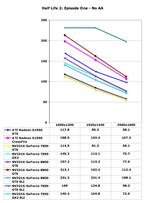
With 4xAA, Episode One showed a bit more separation, and our particular demo seemed to be CPU limited to around 230 FPS. Disabling antialiasing shows that 230 FPS is indeed where our CPU tops out. The other cards move closer to this mark, but without dropping to a lower resolution none of them are yet able to reach it. With the minimum score coming in at 56 FPS, and even then only at 2560x1600, Half-Life 2: Episode One does not appear to really need anything faster in the GPU department just yet.
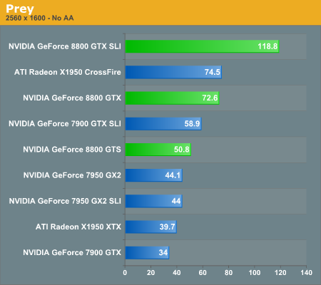
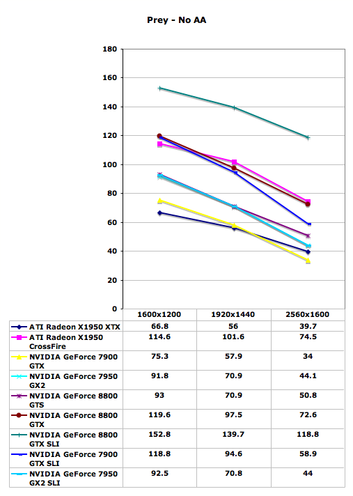
Disabling antialiasing in Prey improved performance in most of the tested configurations by about 20%, and the 8800 GTX SLI setup becomes a bit more CPU limited.. The relative positions of the cards don't really change much, although the GeForce 7 series cards appear to do slightly better without antialiasing compared to the ATI cards.
Final Words
Back when Sony announced the specifications of the PlayStation 3, everyone asked if it meant the end of PC gaming. After all Cell looked very strong and NVIDIA's RSX GPU had tremendous power. We asked NVIDIA how long it would take until we saw a GPU faster than the RSX. Their answer: by the time the PS3 ships. So congratulations to NVIDIA for making the PS3 obsolete before it ever shipped, as G80 is truly a beast.
A single GeForce 8800 GTX is more powerful overall than a 7900 GTX SLI configuration and even NVIDIA's mammoth Quad SLI. Although it's no longer a surprise to see a new generation of GPU outperform the previous generation in SLI, the sheer performance we're able to attain because of G80 is still breathtaking. Being able to run modern day games at 2560x1600 at the highest in-game detail settings completely changes the PC gaming experience. It's an expensive proposition, sure, but it's like no other; games just look so much better on a 30" display at 2560x1600 that it makes playing titles at 1600x1200 seem just "ok". We were less impressed by the hardware itself than by gaming at 2560x1600 with all the quality settings cranked all the way up in every game we tried, and that is saying quite a lot. And in reality, that's what it's all about anyway: delivering quality and performance at levels never before thought possible.
Architecturally, G80 is a gigantic leap from the previous generation of GPUs. It's the type of leap in performance that's akin to what we saw with the Radeon 9700 Pro, and given the number of 9700 Pro-like launches we've seen, they are rare. Like 9700 Pro, we are able to enable features that improve image quality well beyond the previous generation, and we are able to run games smoothly at resolutions higher than we could hope for. And, like 9700 Pro, the best is yet to come.
With developers much more acclimated to programmable shader hardware, we expect to see a faster ramp in the availability of advanced features enabled by DirectX 10 class hardware. This is more because of the performance improvements of DX10 than anything else: game developers can create just about the same effects in SM3.0 that they can with SM4.0. The difference is that DX9 performance would be so low that features won't be worth implementing. This is different from the DX8 to DX9 transition where fully programmable shaders enabled a new class of effects. This time, DX10 simply removes the speed limit and straps on afterburners. The only fly in the ointment for DirectX 10 is the requirement that users run Windows Vista. Unfortunately, that means developers are going to be stuck with supporting both DX9 and DX10 hardware in their titles for some time, unless they simply want to eliminate Windows XP users as a potential market.
Much of the feature set for G80 can be taken advantage of through OpenGL on Windows XP today. Unfortunately, OpenGL has fallen out of use in games these days, but there are still a few who cling to its clean interface and extensibility. The ability to make use of DX10 class features is here today for those who wish to do so.
That's not to say that DX9 games won't see benefits from NVIDIA's new powerhouse. Everything we've tested here today shows incredible scaling on G80 and proves that a unified architecture is the way to go forward in graphics. More complex SM3.0 code will be capable of running on G80 faster than we've been able to see on G70 and R580, and we certainly hope developers will take advantage of that and start releasing games with the option to enable unheard of detail.
The bottom line is that we've got an excellent new GPU that enables incredible levels of performance and quality. And NVIDIA is able to do this while using a reasonable amount of power for the performance gained (despite requiring two PCIe power connectors per 8800 GTX). The chip is huge in terms of transistor count, and in terms of die area. Our estimates based on the wafer shots NVIDIA provided us with indicate that the 681 million transistor G80 die is somewhere between 480 and 530 mm^2 at 90nm. This leaves NVIDIA with the possibility of a spring refresh part based on TSMC's 80nm half-node process that could enable not only better prices, but higher performance and lower power as well.
While we weren't able to overclock the shader core of our G80 parts, NVIDIA has stated that shader core overclocking is coming. While playing around with the new nTune, overclocking the core clock does impact performance, but we'll talk more about this in our retail product review to be posted in the coming days.
With G80, NVIDIA is solidly in a leadership position and now we play the waiting game for ATI's R600 to arrive. One thing is for sure, if you were thinking about building a high end gaming system this holiday season, you only need to consider one card.

