
Original Link: https://www.anandtech.com/show/2381
ASUS P5E3 Deluxe Overclocking: DDR3 Takes Front Stage
by Kris Boughton on November 20, 2007 4:00 AM EST- Posted in
- CPUs
Back in September we published an early first look of the ASUS P5E3 Deluxe motherboard. Based on the Intel X38 chipset, this feature-rich board provided us with the promise of good things to come. Unfortunately, rumors surrounding Intel's unexpected problems with the production and distribution of their newest performance desktop chipset were correct and prevented us from going into much more detail. We ended our preliminary examination with the promise of revisiting the board at a not-so-distant date. Our hope was that our patience in the matter would ultimately bestow upon us - first-hand - the benefits of more mature BIOS releases.
Regrettably, not much has changed in regards to the performance of the X38, although the last few weeks have given us the chance to thoroughly explore the BIOS and map some of the rather elusive feature options to improve performance. At this stage, we are finally comfortable with the X38 chipset and believe it has plenty of hidden performance potential if you know where to look for it. In truth, ASUS has given considerable attention to improving the board's BIOS functionality, but quantifying these differences can be a challenge.
In the end, it is difficult to unlock massive amounts of hidden performance when it's just not there. One thing's for certain though, motherboards based on the X38 chipset that make use of older DDR2 technology will never reach the same levels of performance we are starting to see with the DDR3 boards. A quick scan of current DDR3 memory and motherboard prices should be enough to convince just about anyone that upgrading today is serious business.
 |
The last few weeks have presented many enthusiasts with the opportunity to catch their breath; having just experienced the P35 launch last spring, they now have to decide whether to go the X38/X48 and DDR3 route. Deciding whether to make the change to DDR3 is not very difficult: you can afford the buy-in, or you cannot. Given the choice, especially considering the rate at which DDR2 prices continue to plummet, it should come as no surprise that a large majority of users will probably find themselves in a rather favorable situation - one in which the benefits of staying with DDR2 for a little while longer make too much sense to move at this point.
Of course, it's fair to point out that it is common for the market to endure a period of significant buyer hesitation associated with the adoption of new products or technology - usually attributed to a general unfamiliarity with the benefits that come from purchasing the new technologies. As bleeding edge enthusiasts carrying enough credit card debt to send the stock market spiraling downward, we find it hard to stick with DDR2, even though this would be the wise decision at this point. However, after using DDR3 for the past few months, we find it difficult to go back for several reasons, the primary one being our ever-increasing thirst for improving the performance of our shiny new Penryn based processors.
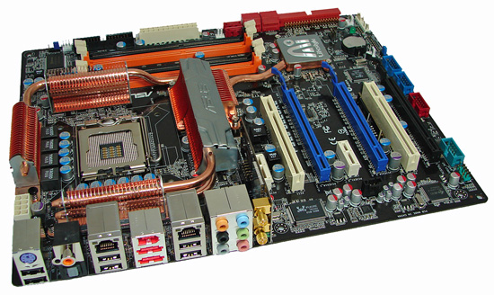
True to fashion, ASUS has once again taken center stage, having worked hard to deliver the P5E3 Deluxe quickly into the hands of salivating enthusiasts. Competition for the title of "world's greatest overclocking motherboard" is fierce, often times having no clear winner. The measured performance margin between close competitors is frequently trivial enough that the tough decision regarding which board to buy comes down to nothing more than personal preference, even brand loyalty. This particular performance segment is exceedingly narrow though, as the number of DDR3-flavored X38 boards for the overclocker is limited at this time.
Those that find themselves entirely unfamiliar with the ASUS P5E3 Deluxe general feature set would do well to check out our first look at this capable board. This time around, we will be taking a detailed look at overclocking capabilities, specifically memory scaling and the effect on overall performance. Before we do this though, let us take a second look at the general board features and layout. We will also point out a few of the hardware features ASUS includes in an effort to improve the motherboard's ability to deliver a strong and stable overclock for Intel's latest processors.
Board Layout and Features
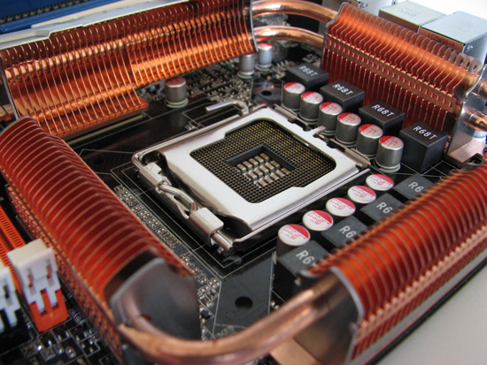 |
ASUS decided to surround the LGA775 socket on all four sides with a generous portion of copper heatpipe-pierced heatsinks, in effect thermally adjoining the memory control hub (MCH) and both sets of power MOSFET banks. The portion of the cooler located between the CPU socket and memory DIMMs is "floating" above the board with a thin layer of electrically insulating material isolating it from the components below. As is usually the case, the stock mounting solution does not provide enough clamping pressure, resulting in increased thermal resistance that usually leads to higher component temperatures than would normally be experienced. We noticed this same problem on the abit IP35-Pro, although the ASUS design did provide better overall cooling.
The P5E3 Deluxe makes excellent use of an 8-phase power delivery system, a must for any board engineered to provide the high current required when pushing a quad-core processors well beyond stock speeds. Although the MOSFETs are completely capable of operating without issue over an exceptionally large temperature range (often able to survive temperatures reaching 120C or greater) it is the Northbridge (MCH) that we really worry about. Our testing has shown the X38 chipset to be particularly sensitive to sustained load temperatures in excess of about 50-55C.
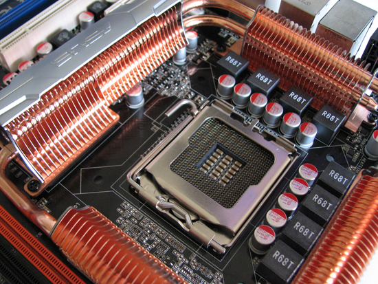 |
The solution to correcting the lackluster mounting pressure was almost effortless (making us wonder why ASUS didn't make the extra effort and save us the trouble). We simply removed any hardware holding the heatpipe assembly to the board, cleaned all thermal surfaces with rubbing alcohol (making sure we allowed ample time for the board to completely dry), and then remounted the unit with a fresh coating of our favorite thermal paste. This time we used small machine screws and threaded nuts in place of the plastic pushpins. This allowed us to control the loading pressure, ensuring a secure bond between the copper and the heat sources. Looking at the picture above, please note the black replacement screws used to hold everything together. In the end, the effort we invested in improving our board's cooling efficiency resulted in more than an 8C drop in measured MCH load temperatures.
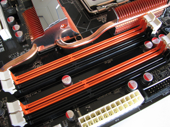 |
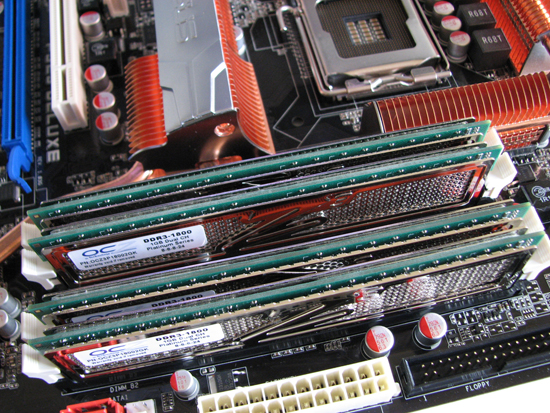
As we can see, ASUS has done a wonderful job of physically locating the DIMMs as close as possible to the MCH in an effort to minimize trace lengths and maximize overclocking potential. When combined with new design features on DDR3 modules, like fully terminated data and address signal lines and 2-phase power from the motherboard, these small changes can result in rather massive increases in memory operating frequencies with low voltages.
The X38 MCH provides official support for up to 8GB of low-voltage DDR3, meaning even the most memory intensive application running atop Windows Vista 64-bit should be happy. The primary 24-pin power connector is located on the bottom edge of the board with the supplementary 8-pin EPS12V power connector being located at the top of the board near the backplane.
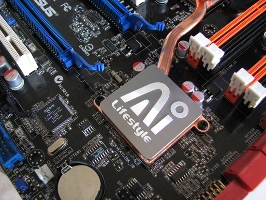 |
Intel's ICH9R, although rated at no more than about 6W when operating, is connected to the stock board cooling solution using a single heatpipe - no doubt, we discovered the Southbridge heatsink is hotter for this very reason than it otherwise would be. The board provides six SATA ports, more than enough for most overclockers. Unfortunately, ASUS decided not to include an LED POST code reader somewhere making it difficult to determine exactly what the board is doing during the POST period.
The small blue header to the bottom of the board is used for clearing the BIOS should the need arise. We were pleasantly surprised as to how gracefully the board recovered from a failed setting - one quick full-power cycle and the board defaulted to safe settings allowing us to easily enter the BIOS and correct our mistake.
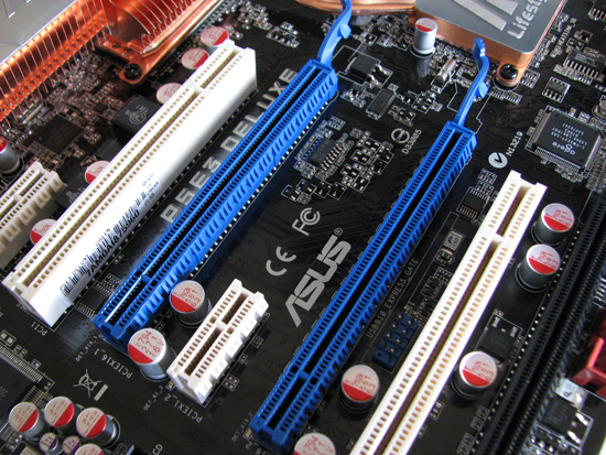 |
One of the features separating the X38 chipset from the mainstream segment P35 MCH is the addition of PCI-E 2.0 specification compatibility. The blue slots connect direct to the MCH and each provides the full 16 lanes of bandwidth - though truthfully, we can't see the additional bandwidth really helping much as PCI-E throughput often isn't the limiting factor, especially with PCI-E 2.0 already doubling the bandwidth for 1.x. The third x16 slot (black) can operate at either x1 or x4 speeds. Two PCI slots and one additional PCI-E x1 slot round out the board's expansion capabilities.
Test Setup and Overclocking Results
| ASUS P5E3 Deluxe Overclocking Testbed |
|
| Processor | Intel Core 2 Quad Q6600 Quad-core, 2.4GHz, 8MB Unified Cache, 9x Multiplier, 1066FSB |
| CPU Voltage | 1.2750v Stock |
| Cooling | D-tek FuZion CPU water block, EK FC8800-GTX/Ultra full coverage GPU block, Thermochill PA120.3 radiator, dual Laing D5 pumps in series, 1/2" ID (3/4" OD) Tygon tubing, 6x Yate Loon D12SM-12 120x25mm fans @ 12v in push/pull configuration |
| Power Supply | Seasonic 600W |
| Memory | OCZ DDR3 PC3-14400 (DDR-1800) Platinum Edition |
| Memory Settings | 4-4-4-12 (DDR-1066) to 8-8-8-15 (DDR-1940) |
| Video Cards | MSI 8800 Ultra (660/1050) |
| Video Drivers | NVIDIA 164.09 (beta) |
| Hard Drive | 2x Western Digital 10K RPM 74GB SATA 3/Gbps 8MB Buffer (RAID 0) |
| Optical Drives | 2x Plextor PX-755A |
| Case | Lian-Li PC-G70B |
| BIOS | ASUS 0601 |
| Operating System | Windows XP Professional SP2 |
We decided to make our first overclocking results available using a Q6600 quad-core as we feel this chip is great for the mainstream desktop performance crowd and is widely available at an attractive price. We chose high performance DDR3 in order to highlight the board's memory performance capabilities. Because testing was completed using a 32-bit operating system, we decided to limit ourselves to a maximum of 2GB memory for our initial results. Future testing on this board, including tests run using Windows Vista 64-bit, will utilize up to 4GB of the same DDR3 memory.
We used water-cooling in place of typical air-cooling. This assured us that performance limitations due to excessive CPU temperatures would not be a problem during multiple testing runs. Pushing a 65nm quad-core past 3.6GHz requires a robust cooling system in order to maintain system stability during periods of heavy benchmarking. Furthermore, our cooling system makes use of redundant components where possible to account for the potential failure of critical cooling components (i.e. two pumps, etc).
Standard benchmarks included 3DMark06 (at the default 1280x1024 resolution) for testing overall graphics performance and Super PI 32M for combined processor/memory testing as well as CineBench10 and WinRAR 3.70 (a great way to quickly measure memory system performance). We utilized EVEREST 4.20 extensively in the collection and analysis of synthetic memory performance benchmarks (memory read and overall memory latency).
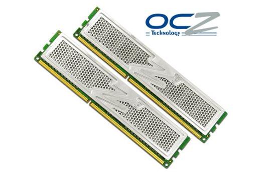
With the motherboard picked out all we had left to do was choose a pair of 1GB DDR3 modules. We decided on a pair (2x1024MB) of OCZ DDR3 PC3-14400 (DDR-1800) Platinum Edition modules, which proved to be tremendously capable across an amazing range of frequencies and timings. This allowed us the flexibility we needed to perform direct performance caparisons at legacy DDR2 speeds as well as the overclocking headroom we craved. Cool to the touch during even the most intense benchmarking session and exceptionally responsive to voltage on the test bench, these modules are great choices for those looking to overclock.
Now that we have looked at our test setup and gone over a few of the ways that we intend on measuring our system's performance, let us explore the ASUS P5E3 Deluxe BIOS options.
ASUS P5E3 Deluxe BIOS Setup and Tweaking
Of all the board manufacturers, ASUS seems to have captured the market on the use of proprietary names for several of their BIOS functions. The first order of business is to understand what it is we will be manipulating (hopefully for the better). The best way to go about this is to lay it all out and go straight down the list. We will do our best to explain what ASUS is trying to convey with their particular naming scheme, what the settings actually change, and finally, when you want to make use of each setting.
Ai Tweaker Menu
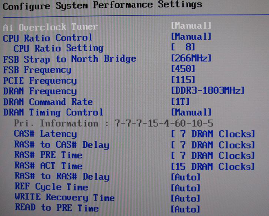
Ai Overclock Tuner: Auto, Manual, and XMP. Auto runs the board at default (optimal) settings with no overclock, Manual allow the user to set each individual overclocking parameter and XMP instructs the board to attempt to set CPU and MCH parameters as necessary in order to configure the system to operate the memory as defined by one of the memory's pre-programmed eXtreme Memory Profiles.
eXtreme Memory Profile, or XMP, is Intel's version of the same experience offered by NVIDIA's EPP (Enhanced Performance Profile), in which memory overclocking settings - including frequency, timings, and voltages - are programmed into the memory module's SPD chip. Assuming the CPU is capable of supporting the profile, selecting either Profile #1 or Profile #2 (as they exist) gives the user an easy way to experience overclocking without getting too involved in the setup process.
After selecting Manual the following options become available for change:
CPU Ratio Control: Auto and Manual. Selecting Manual allows for altering the CPU's operating multiplier. Leaving this set to Auto instructs the BIOS to use the CPU's default multiplier, or in the case of XMP operation, to select a multiplier that would most closely maintain the default CPU frequency when automatically overclocking the memory.
CPU Ratio Setting: Available options range from 6 to the installed CPU's default multiplier (in the case of the Q6600 this would be 9). Extreme-series CPUs (QX6850, QX9650, etc.) are also upwards unlocked and can be set as high as 31x.
FSB Strap to Northbridge: Auto, 200, 266, 333, and 400. There once was a time when this single setting controlled a whole series of MCH performance configuration registers. Implemented in its current form, this option does little more than determine what memory dividers are available for use. Lower straps can impose early front side bus (FSB) limitations - if you experience problems, choose the next higher strap and select the appropriate divider to keep your memory frequency at an achievable target. The general practice when overclocking is to keep the strap as low as possible after setting an acceptable CPU and memory speed. The P5E3 seems to break this wisdom and often performs best using the 333 strap regardless of FSB speeds.
| Memory Divider Ratios Available by FSB Strap (DRAM:FSB) | |
| 200 | 5:3, 2:1 |
| 266 | 5:4, 3:2, 2:1 |
| 333 | 1:1, 6:5, 8:5, 2:1 |
| 400 | 1:1. 4:3, 3:2, 2:1 |
FSB Frequency: This value, when multiplied by the CPU Ratio Setting, sets the processor frequency. For example, 400 FSB x 9 = 3.6GHz. This setting, along with the FSB Strap to Northbridge, influences what DRAM Frequency(s) are available for selection. (Most 65nm quad-cores are FSB limited by this board to around 480-500MHz without serious tweaking and voltages.)
PCI-E Frequency: Set no higher than 115-118MHz and you may see a small increase in 3D game/benchmark performance. Exceeding this recommendation will cause problems with the Southbridge to Northbridge DMI interface making it appear as though attached peripherals, including hard disk drives, have failed.
DRAM Frequency: Choose from those listed to set the system DDR memory frequency. Altering the FSB Frequency or FSB Strap to Northbridge settings will influence the selections available. Refer to the table above when targeting a specific memory speed. For example, if the 333 strap is selected with an FSB setting of 400 then the list would contain the following selection choices: 2 x 400 FSB x 1/1 = DDR-800, 2 x 400 FSB x 6/5 = DDR-960, 2 x 400 FSB x 8/5 = DDR-1280, and 2 x 400 FSB x 2/1 = DDR-1600.
DRAM Command Rate: Auto, 1T, and 2T. Incorrectly labeled as 1T and 2T, these settings are really 1N and 2N, as implemented by the Intel X38 MCH. Auto allows the BIOS to assign the value automatically based on FSB Strap to Northbridge and final memory frequency. In most cases, system stability is not affected and a 3-5% improvement in memory bandwidth boost is available when set to 1N.
DRAM Timing Control: Auto and Manual. Auto allows the BIOS to read and set all primary and secondary timings for the installed memory as detailed by SPD. Manual gives the user control over individual memory timings while allowing the option of having some timings remain automatically assigned based on programmed values. In most cases the only timings that need to be manually configured are: CAS# Latency (tCL), RAS# to CAS# Delay (tRCD), RAS# PRE Time (tRP) and RAS# ACT Time (tRAS) - leave all others sub-timings set to Auto unless you have a good reason for changing them.
BIOS Setup and Tweaking, Continued
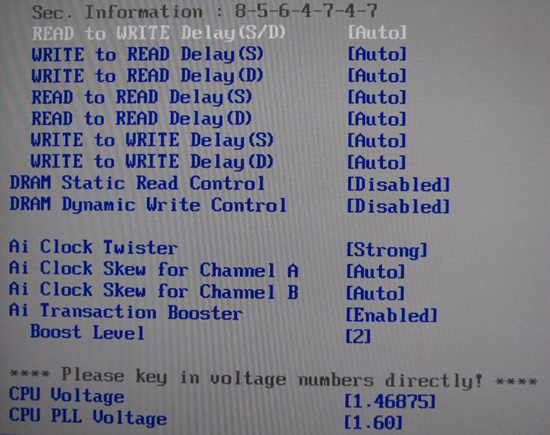
DRAM Static Read Control: Auto, Enabled, and Disabled. We were unable to affect any measurable performance change because of toggling this setting. This setting is curious by its very nature as Ai Transaction Booster (explained below) manipulates the MCH Static Read Control Delay setting directly, implying there would be no reason for this option.
DRAM Dynamic Write Control: Auto, Enabled, and Disabled. See above.
Ai Clock Twister: Auto, Light, Moderate, and Strong. This setting controls the number of memory access phases that are "pulled-in" to the next lower (higher performance) Static Read Delay value. In essence, this allows for smaller, incremental performance gains if the user is unable to achieve stability when using the next lower Static Read Delay value.
Ai Clock Skew for Channel A/B: This setting allows you to either advance or delay the signal timings for Channel A or Channel B DIMMs. Because it's not possible to locate all memory modules an equal distance from the MCH, it's important to be able to adjust signal timing to ensure all data (or requests for data) arrive at the same point at precisely the same time. When experimenting with this setting either slightly delay Channel A (since it's closer to the MCH) or advance Channel B - do not change both simultaneously unless you find you need more than 350ps (picoseconds) of total skew (highly unlikely).
Ai Transaction Booster: Auto, Enabled (Boost: 1-8), and Disabled (Relax: 1-8). This is probably one of the most important BIOS settings when it comes to extracting every possible bit of performance from the system. Setting these fields can improve total memory bandwidth up to 15% and produce a considerable reduction in access latency.
Static Read Control Delay, sometimes referred to as Performance Level, is a primary MCH "timing" value and has a rather significant impact on memory read performance as well as overall memory access latency. In case you are wondering why low access latency matters, we submit to you the following quick-and-dirty response: improved memory latency (courtesy of the Integrated Memory Controller/IMC) is the primary reason that AMD Athlon 64 chips have performed so well. Latency is one of the few areas where AMD maintains a lead over Intel, and Intel will move to an IMC design late next year (starting with Nehalem).
Much like primary memory timings, this MCH "timing" is measured in clock cycles and is relative to the base transmission frequency (2 x FSB). This explains why Static Read Control Delay should increase as FSB rates rise. Similar to memory timings, maintaining a lower value longer with the proper application of MCH voltage can lead to improved performance. In other words, "boosting" the Ai Transaction level may require a higher MCH voltage than would be otherwise required if a more relaxed level were set.
Because these settings effectively apply an offset to the default value it can sometimes be difficult to confirm exactly what is going on - it is almost like flying blind. Thankfully, a wonderful tool exists that reads and reports "Performance Level" from within Windows, allowing us to verify that the board is operating as intended. Memset 3.4 (beta 3), available as freeware, can be found through a simple search using your favorite search engine. Here we see Performance Level, as reported by Memset 3.4, as well as Command Rate and memory latency from EVEREST 4.20.
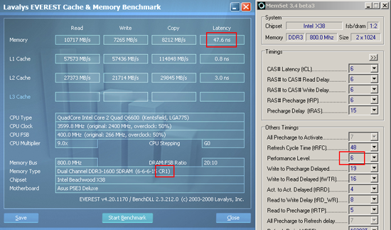 |
Auto allows the BIOS to set the values automatically which, through simple experimentation and observation, has been simplified to the following relationship: Static Read Control Delay (default) = tCL. Knowing this makes adjusting the value rather simple. Keep in mind that workable values are in the range of 1-3 (boost or relax) only; selecting values from 4 through 8 will always result in a POST failure.
For example, with memory set to DDR-1600 6-6-6-15, the BIOS will establish a default Static Read Control Delay of 6. Setting Ai Transaction Booster to Enabled with a Boost Level of 1 results in a final Static Read Control Delay setting of 6 - 1 = 5. Alternatively, selecting Disabled with a Relax Level of 1 results in a final value of 6 + 1 = 7. Just like in the case of memory timings, lower is tighter (higher performance).
Finally, a simple rule to keep in mind when setting Static Read Control Delay - 4 requires a CAS Latency (tCL) of 6 or lower, 5 requires a tCL of 7 or lower, and 6 requires a tCL of 8 or lower. There are no other known limitations at this time.
CPU Voltage: Maximum of 1.7000V. Our experience with the ASUS P5E3 Deluxe has shown a rather large voltage offset when it comes to VCore. For example, setting 1.4675V in the BIOS results in an in-Windows idle voltage of ~1.4250V by DMM. Under load we see the voltage settle out as low as 1.39V. While we understand the need and requirement for VDroop, a total difference in programmed BIOS voltage to full-load voltage of more than 0.07V is excessive. Keep this in mind when setting this value if you already know the minimum voltage your CPU needs for stable operation or utilize the load-line calibration setting listed below to reduce VDroop.
CPU PLL Voltage: Maximum of 2.78V. Out of all the voltages the user can manipulate this one is by far the most dangerous. Maximum vCPUpll, as established by Intel, is 1.60V (default for this board) making 2.78V a whopping ~75% over specification! (As an aside, this would be the equivalent of subjecting your 65nm CPU to a core voltage of over 2.5V). Exercise extreme caution when utilizing higher values as setting this value too high can result in the CPUs "losing cores" after being subjected to voltage in excess of ~2.0V. The good news is that we did not see an increase in overclocking potential with voltages above 1.68V.
More BIOS Setup and Tweaking
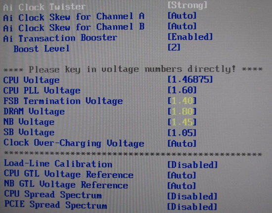
FSB Termination Voltage: Maximum of 1.50V. Undeniably the Achilles' heel of this fine board, 1.5V (VTT) is simply not enough to carry most 65nm quad-cores above ~500MHz FSB. Most CPUs/MCHs require this voltage to quickly ramp up from the default (1.20V) to near maximum when overclocking from about 450MHz FSB and higher.
DRAM Voltage: Maximum of 2.78V. Base DDR3 voltages are set to 1.5V with most performance kits requiring somewhere between 1.8V and 1.95V. Our recommendation is never to exceed the manufacturer's maximum specified voltage. With that said, values in excess of ~2.2V with DDR3 are a death sentence. In light of this, allowing a voltage as high as 2.78V seems irresponsible but is a required marketing feature.
NB Voltage: Maximum of 1.91V. NB Voltage, also known as VMCH, is an integral part of high-FSB overclocking, especially when running a "boosted" Ai Transaction Booster level. Maximum FSB achieved with a 65nm quad-core was around ~1.75V VMCH. Voltages above 1.75V, being excessive, will more than likely accelerate the failure of your board and cause unneeded heating of the MCH die.
Certain instabilities arose when running Northbridge voltages in excess of ~1.75V, caused by high internal die temperatures because of the voltage. Simply lowering VMCH was enough to return to stable operation. We've also found that the X38 chipset is far more sensitive to heat than any other Intel chipset to date. In fact, the BIOS is kind enough to warn the inexperienced user that Northbridge voltages in excess of 1.75V require a more effective cooling solution as the stock heatsink and heatpipe assembly can only do so much.
SB Voltage: Maximum of 1.20V. Some users have claimed that a higher Southbridge voltage provides for additional stability when running the PCI-E frequency out of specification. We have found leaving this voltage on Auto as the most appropriate solution, even when overclocking.
Clock Over-Charging Voltage: Maximum of 1.00V. Phase change, dry ice (DI) and liquid nitrogen (LN2) benchers may find higher settings here useful when cooling the CPU and surrounding area down to very low levels. All others would do best to leave this on Auto.
Load-Line Calibration: Acts to reduce the affects of VDroop during periods of heavy CPU loading. Enabling Load-Line Calibration may allow you to set a lower CPU Voltage in the BIOS while retaining overall system stability.
CPU/NB GTL Voltage Reference: CPU: Auto, 0.63x, 0.61x, 0.59x, and 0.57x. NB: Auto, 0.67x, and 0.61x. CPU Gunning Transceiver Logic (GTL) voltages are nothing more than reference levels that the CPU uses when determining if a data or address signal is either high (1) or low (0). Precision voltage dividers generate these voltages and are usually specified as a percentage of VTT. In the case of 0.67, this would be 67% of VTT. For example, if VTT is 1.20v then a CPU GTL Voltage Reference of 0.67x would result in a GTLREF value of 0.67 x 1.20V = ~0.80V.
These reference values are particularly important when overclocking quad-core CPUs, especially when venturing above about 450FSB. The ability to tune these values per die can mean the difference between 475FSB and 500FSB. Unfortunately, ASUS' implementation of this functionality is rather incomplete as manipulation of only a single GTLREF value is possible (and in a somewhat imprecise manner). The real power in GTLREF tuning comes in the ability to provide each quad-core die with separate reference values. (Recall that current quad-cores are an MCM consisting of two dual-core dies on a single package.) Unfortunately, this is not a matter of future BIOS modification as providing two distinct voltages to separate pins on the CPU would require nothing less than a PCB revision. As such, this board will most likely never see its full potential when clocking quad-core CPUs but it still performs admirably.
This same information applies to the NB GTL Voltage Reference setting except that there is no need for more than one reference value. In the case of each, we would like to see much finer control of these values. Ironically, the board's controllable voltages that need the least amount of precision seem to have the most. However, ASUS is working on these requests for their next boards; in the meantime, unless you push the board past about 98% of its maximum, these shortcomings will not affect the typical user of this board. We might add that other manufacturers face the same problem.
CPU/PCIE Spread Spectrum: Set both to Disabled for a more stable clocking signal.
450 FSB Quad-Core BIOS Settings
In the true spirit of giving we present to you an easy, all-in-one overclock setting guide, practically guaranteed to have your 65nm quad-core stable at 450MHz FSB or greater. You may find the need to increase the voltage for your particular CPU higher than our suggestions if cooling permits.
| ASUS P5E3 Deluxe Quad-Core Setup Guide for 450FSB | |
| CPU Features | |
| Ai Overclock Tuner | Manual |
| CPU Ratio Control | Manual |
| CPU Ratio Setting | 8 |
| FSB Strap to North Bridge | 266 |
| FSB Frequency | 450 |
| PCIE Frequency | 115 |
| DRAM Frequency | DDR-1800 |
| DRAM Command Rate | 1T |
| DRAM Timing Control | Manual |
| DRAM Timings | |
| CAS# Latency | 7 DRAM Clocks |
| RAS# to CAS# Delay | 7 DRAM Clocks |
| RAS# PRE Time | 7 DRAM Clocks |
| RAS# ACT Time | 15 DRAM Clocks |
| RAS# to RAS# Delay | Auto |
| REF Cycle Time | Auto |
| WRITE Recovery Time | Auto |
| READ to PRE Time | Auto |
| READ to WRITE Delay(S/D) | Auto |
| WRITE to READ Delay(S) | Auto |
| READ to READ Delay(S) | Auto |
| READ to READ Delay(D) | Auto |
| WRITE to WRITE Delay(S) | Auto |
| WRITE to WRITE Delay(D) | Auto |
| DRAM Static Read Control | Disabled |
| DRAM Dynamic Write Control | Disabled |
| Ai Clock Twister | Strong |
| Ai Clock Skew for Channel A | Auto |
| Ai Clock Skew for Channel B | Auto |
| Ai Transaction Booster | Enabled |
| Boost Level | 2 |
| Voltage Settings | |
| CPU Voltage | 1.475 |
| CPU PLL Voltage | 1.6 |
| FSB Termination Voltage | 1.5 |
| DRAM Voltage | 1.96 |
| NB Voltage | 1.61 |
| SB Voltage | Auto |
| Clock Over-Charging Voltage | Auto |
| Load-Line Calibration | Disabled |
| CPU GTL Voltage Reference | Auto |
| NB GTL Voltage Reference | Auto |
| CPU Spread Spectrum | Disabled |
| PCIE Spread Spectrum | Disabled |
General Memory Performance Scaling and Command Rate
Fiddling with the BIOS to see what works and what does not is all well and good but meaningless unless we have A way to quantify the results. To that end, we've done our best to tabulate the details of our testing and present the following.
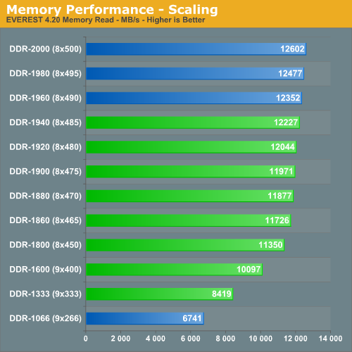
Before delving into more advanced discussions let's first review what we already know about typical memory scaling. In this graph, we show how memory responds to a simple change in base operating frequency. Here we can see the memory responds just as we expect - higher frequencies bring about higher bandwidths.
The green lines represent actual data points, collected with timings of 8-8-8-15, a Static Read Control Delay of 7 and Command Rate 1N. The blue lines represent extrapolated data points - i.e. we did not measure these values directly but rather scaled existing test results to create additional information for comparison purposes. This is an important detail to note as this means we extrapolated the data points in the context of our original tests (the same timings, etc.). While this isn't 100% accurate, it does provide a very good estimate for the timings you would most likely set at these particular speeds.
The result is an unadulterated illustration of memory read performance with frequency being the only variable - just as we intended. This also gives us the ability to predict how our memory would perform should we run it at DDR-2000 with 8-8-8-15 timings. While some choose to do this by pumping excessive voltage through their memory modules, we feel our method is safer as we do not risk damaging our expensive DDR3. Future DDR3 will likely be able to reach these higher performance settings at more reasonable voltages, however.
Our ASUS P5E3 Deluxe exhibited an amazing memory scaling range, allowing us to run our memory 1:1 at stock speeds with tight 4-4-4-12 timings and as high as about DDR-1960 at 8-8-8-15 by using the more exotic 2:1 divider. It appears our final limitation was the board/CPU combination and not the memory. We have no doubt the memory would have continued to scale well above 2GHz had there been additional FSB headroom to play with.
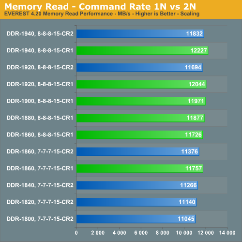
In this analysis, intended to show the affect of 1N versus 2N Command Rate, we see that setting 1N (DRAM Command Rate to 1T) can improve synthetic memory read scores by as much as ~3.3% over 2N. Static Read Control Delay was held constant at 7 through the use of Ai Transaction Booster while both DDR3 memory frequency and timings were increased and Command Rate was forced to either 1N or 2N by BIOS.
We can conclude that DDR-1860, 8-8-8-15-CR1 is roughly the equivalent of DDR-1925, 8-8-8-15-CR2. This means modules that might not otherwise be able to reach the speeds necessary to provide the desired target bandwidth can take advantage of the performance enhancing capabilities of the MCH in order achieve this end. In most instances enabling Command Rate 1N did nothing to bring about early instability making this setting nothing more than free bandwidth for the taking. The source of the increased bandwidth comes from the addressing efficiency improvements that come with 1N commanding and the reduction in overall memory access latency.
Static Read Control Delay and Latency Considerations
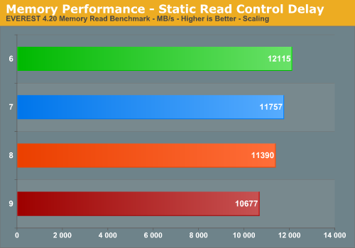
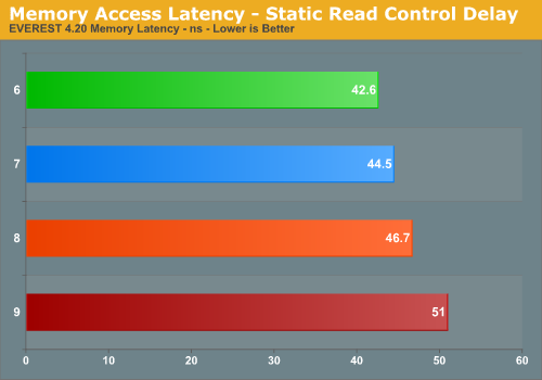
This brings us to the coup de grace of BIOS tweaks - Static Read Control Delay. Only recently discovered and popularized by those looking for every last ounce of memory performance, this tweak is sometimes referred to as Performance Level. Don't let this fool you though; just like golf, lower is better. Tragically, this now-essential setting is among the most misunderstood and often overlooked settings when tuning a board.
In this first graph, we can see the affect of varying the Static Read Control Delay setting. The memory was set to DDR-1860 (8x465) with 7-7-7-15 timings and Command Rate 1N. The difference in performance between the loosest setting of 9 and the tightest setting of 6 is outstanding with nearly a 14% increase in memory read performance without even touching the memory. The second graph demonstrates the equally impressive reduction in overall memory access latency.
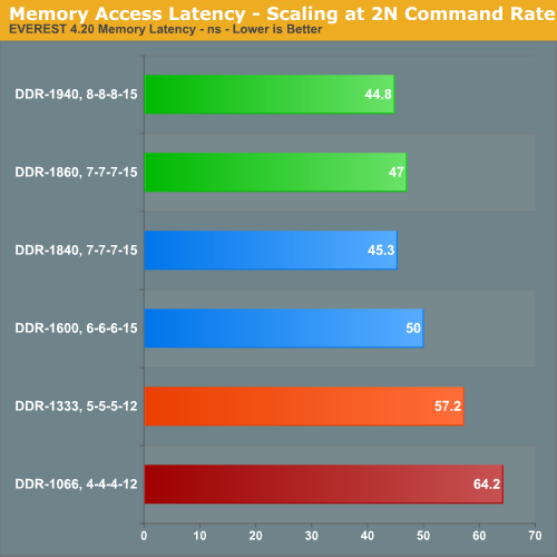
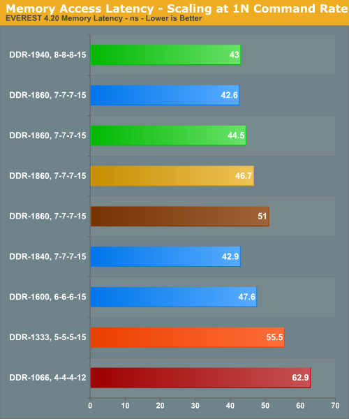
| Memory Access Latency Color Coding Legend | |
| Color | Static Read Control Delay (Performance Level) |
| Red | 4 |
| Orange | 5 |
| Light Blue | 6 |
| Lime Green | 7 |
| Dark Gold | 8 |
| Brown | 9 |
The previous two graphs helps to illustrate both how Command Rate and Static Read Control Delay (Performance Level) influence the overall memory access latency. Notice that the minimum latencies do not occur at the highest memory speed but rather at the higher FSB/DRAM frequency achievable using a Static Read Control Delay of 6. This helps to support our recommendation that 6 should also be your target value when overclocking. Instead of continuing to push the memory harder and harder, forcing more and more voltage into the modules, back off on the frequency until you find the absolute maximum speed that the MCH will run a Static Read Control Delay of 6. Finally, enable Command Rate 1N and tighten the timings as allowable using a voltage with which your components are comfortable - this will usually be the motherboard's sweet spot for performance.
These base settings should provide enough knowledge to tune the ASUS P5E3 Deluxe. In fact, a lot of what we have gone over here translates extremely well too many other Intel X38/P35 motherboards, not just from ASUS but Gigabyte, abit, DFI, etc. The big question on everybody's mind should now be whether any of these tweaks made any difference in real-world performance or in synthetic benchmarks. To answer these questions we first look toward 3DMark06. This particular benchmark does a good job of assessing a system's overall ability to process 3D intensive workloads. At the end of the day, frame rate is still king for gaming.
Overclocking Performance Comparison
All results were taken running memory ratios of 2:1 for final DRAM speeds of DDR-1066 @ 4-4-4-12, DDR-1333 @ 5-5-5-12, DDR-1600 @ 6-6-6-15, and DDR-1860 @ 8-8-8-15, respectively. This way we are able to capture any performance gain possible by taking advantage of the increased memory bandwidth provided by the DDR3 memory. Obviously, the DDR2 used in the testing of the ASUS Maximum Formula SE and the DFI UT P35-T2R needed to make use of lower dividers in order to maintain memory frequency within an achievable range.
Synthetic Graphics Performance
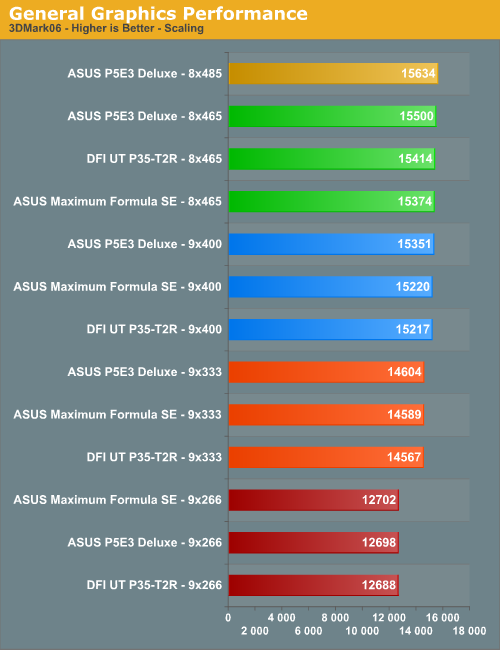
A close examination of the graphics results leads us to believe that, while nice to look at, DDR3 will do little to nothing in improving your overall gaming experience. This should come as no big surprise to anyone as we've known for a while that today's games are very much GPU dependent, especially at higher resolutions. The large performance gain in 3DMark06 seen when overclocking from 9x266 to 9x333 is a strong indication that the system was previously bottlenecked by the CPU when running at the stock 2.4GHz speed. Once we eclipse the 3GHz barrier though we start to see ever diminishing returns as we continue to push the processor higher and higher. This tells us that the system has now become GPU-bound and we can attribute any small gains in scores to the points we gain in the two CPU tests alone. Although the ASUS P5E3 Deluxe did manage to maintain a small lead across all phases of the graphics testing, the difference is hardly sizeable enough to justify the cost of DDR3, although this board will allow you to extract its full potential.
CPU Performance
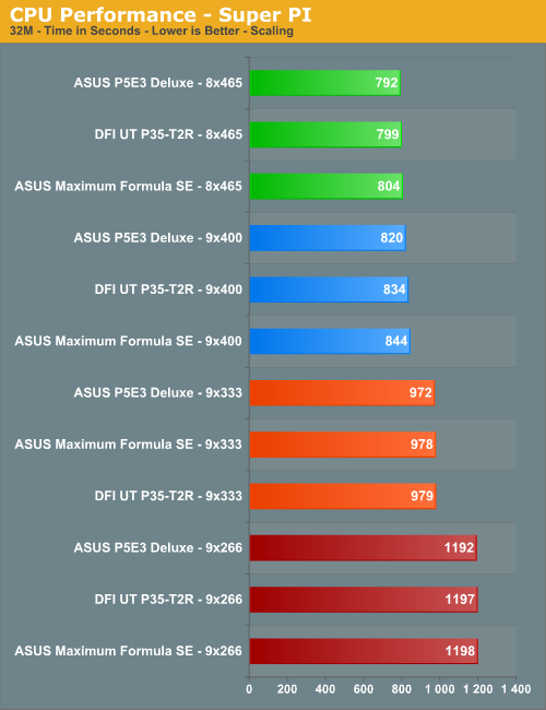
We chose Super PI for testing the CPU/memory subsystem performance. Rather than run short sub-15 second tests that didn't do much to stress the memory we opted to run the longer 32M test. Small gains of approximately 1-3% are hardly groundbreaking. Nevertheless, the ASUS P5E3 Deluxe managed to maintain the performance lead in all test runs. The largest single score improvement was achieved during the 9x400 run with the MCH performance-optimized using a Static Read Control Delay of 6. In this case, tightening the sub-timings and setting Command Rate 1N may have been enough to bring the total time down to less than 800 seconds. We will continue testing this DDR3 and report additional results later.
Rendering Performance
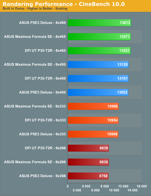
CINEBENCH R10 is a great all-out CPU performance benchmark that scales wonderfully with the number of CPU cores in the system. As such, there is little to no gain seen by running the higher memory speeds provided by our DDR3. We will include Intel 45nm quad-core results in the next article.
File Compression Performance
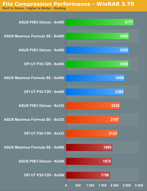
Judging by the results of the built-in file compression benchmark provided in WinRAR 3.70 there is some additional performance available by providing the CPU with additional bandwidth - this makes sense, as file compression is quite data intensive, especially considering the amount of memory flip operations performed by this program. Here we see a solid 7% performance lead by the ASUS P5E3 Deluxe when running at 8x465.
Overclocked Gaming Performance
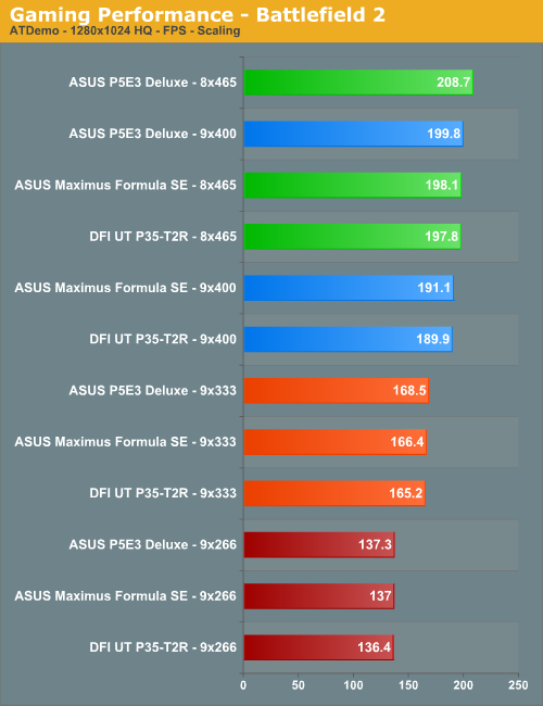
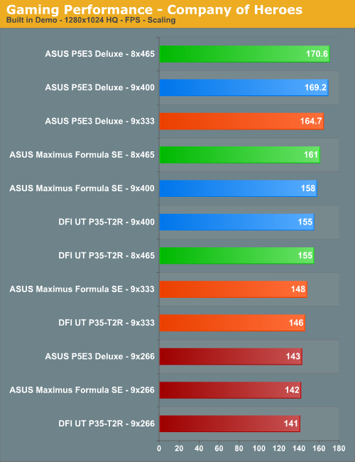
Making use of a somewhat seasoned engine, Battlefield 2 proves once again that good graphics performance isn't always just about high-end graphics cards. Benchmarking at lower FSB levels, where our DDR3 performs more like equivalently binned DDR2, we find similar performance results. However, making use of the superior 2:1 memory divider and running our DDR3 at a full 1.8GHz and higher shows it's rewards. Whereas the ASUS Maximus Formula SE and DFI UT P35-T2R linger just below the 200 FPS mark, the ASUS P5E3 Deluxe proves it has the power to push through this ceiling even while operating at a lower overall CPU speed. Somewhat like Battlefield 2, Company of Heroes shows its ability to make efficient use of the additional bandwidth provided by the ASUS P5E3 Deluxe by quickly becoming GPU limited at around 3GHz on the CPU. Once again, the DDR3 board proves the more capable gaming machine.
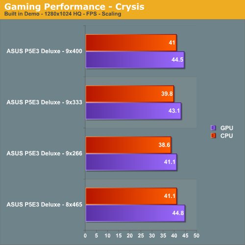
Our third and final gaming performance test involves one of the most highly anticipated releases of all time - Crysis. Until now we were hesitant to provide any benchmarking results based on this engine as our testing policy here at AnandTech generally discourages the use of beta products or pre-release software when categorizing the performance of retail products. With Crysis, the results come from the use of separate CPU and GPU benchmark scripting routines included with the game.
Our Crysis results are both good and bad, depending on how you look at them. The bad news is that our system, consisting of an Intel Q6600 at 3.6GHz (9x400), DDR3 running at DDR-1600, 6-6-6-12 timings, and a single MSI 8800GTX Ultra @ 660/1150 only managed to squeak out an average of ~44 FPS at a rather low resolution of 1280x1024. The good news, of course, is that these numbers didn't seem to change too much even when we dropped the CPU back to the stock 9x266 setting, placing our DDR3 memory squarely in DDR2 territory at DDR-1066, 4-4-4-12. This should give hope to those out there that may not have the most robust hardware available. All Crysis really wants is some serious GPU power.
Conclusion (Part I)
The more time we spend working with DDR3, the more we understand its potential benefits. After spending a week working with memory speeds in excess of 1.8GHz, we find ourselves wondering how we can ever possibly go back to DDR2. Of course, that only lasts until we check our bank accounts. Even though our results may not be enough to truly substantiate such an expensive purchase, we're confident prices will soon begin their descent and DDR3 will eventually find a home in every enthusiast's system. Additionally, while we would like to see a larger performance gain moving from DDR2 to DDR3, as with most top-bin hardware the margin between first and second place is hardly a whisper. Given time to fully mature, DDR3 will become the new de-facto standard in high-performance memory and is something we look forward to, once the costs are no longer prohibitive.
 |
Considering the market placement of the ASUS P5E3 Deluxe, we find the board exceedingly well equipped and capable when placed side-by-side with the usual gambit of competitors. Although not implicitly marketed toward the extreme overclocking crowd, the ASUS P5E3 Deluxe stands its ground and finds a place near the top of our list of favorite overclocking boards. ASUS assures us they are committed to the practice of ongoing support and plan on continuing in their tradition of improvement and innovation with each new BIOS release. In fact, we've already seen several changes in the time that it took to complete this review.
Those that find themselves looking for the ultimate "tweaker" motherboard would do better selecting either the ASUS Maximus Formula/Extreme or the DFI UT P35-T2R. However, what the P5E3 Deluxe lacks in tweaking options it makes up for with performance and features. Check back soon for the second edition (Part II) of our ASUS P5E3 overclocking guide, where we'll be strapping Intel's new Core2 Extreme QX9650 processor into the board and watching for magic to happen as we show how well the new Yorkfield series overclocks.


