Original Link: https://www.anandtech.com/show/2918
At this year’s Consumer Electronics Show, NVIDIA had several things going on. In a public press conference they announced 3D Vision Surround and Tegra 2, while on the showfloor they had products o’plenty, including a GF100 setup showcasing 3D Vision Surround.
But if you’re here, then what you’re most interested in is what wasn’t talked about in public, and that was GF100. With the Fermi-based GF100 GPU finally in full production, NVIDIA was ready to talk to the press about the rest of GF100, and at the tail-end of CES we got our first look at GF100’s gaming abilities, along with a hands-on look at some unknown GF100 products in action. The message NVIDIA was trying to send: GF100 is going to be here soon, and it’s going to be fast.
Fermi/GF100 as announced in September of 2009
Before we get too far ahead of ourselves though, let’s talk about what we know and what we don’t know.
During CES, NVIDIA held deep dive sessions for the hardware press. At these deep dives, NVIDIA focused on 3 things: Discussing GF100’s architecture as is relevant for a gaming/consumer GPU, discussing their developer relations program (including the infamous Batman: Arkham Asylum anti-aliasing situation), and finally demonstrating GF100 in action on some games and some productivity applications.
Many of you have likely already seen the demos, as videos of what we saw have already been on YouTube for a few days now. What you haven’t seen and what we’ll be focusing on today, is what we’ve learned about GF100 as a gaming GPU. We now know everything about what makes GF100 tick, and we’re going to share it all with you.
With that said, while NVIDIA is showing off GF100, they aren’t showing off the final products. As such we can talk about the GPU, but we don’t know anything about the final cards. All of that will be announced at a later time – and no, we don’t know that either. In short, here’s what we still don’t know and will not be able to cover today:
- Die size
- What cards will be made from the GF100
- Clock speeds
- Power usage (we only know that it’s more than GT200)
- Pricing
- Performance
At this point the final products and pricing are going to heavily depend on what the final GF100 chips are like. The clockspeeds NVIDIA can get away with will determine power usage and performance, and by extension of that, pricing. Make no mistake though, NVIDIA is clearly aiming to be faster than AMD’s Radeon HD 5870, so form your expectations accordingly.
For performance in particular, we have seen one benchmark: Far Cry 2, running the Ranch Small demo, with NVIDIA running it on both their unnamed GF100 card and a GTX285. The GF100 card was faster (84fps vs. 50fps), but as Ranch Small is a semi-randomized benchmark (certain objects are in some runs and not others) and we’ve seen Far Cry 2 to be CPU-limited in other situations, we don’t put much faith in this specific benchmark. When it comes to performance, we’re content to wait until we can test GF100 cards ourselves.
With that out of the way, let’s get started on GF100.
GF100’s Gaming Architecture
Although it feels like ages ago, NVIDIA announced the Fermi architecture back in September of 2009, focusing on the compute abilities of the GPU that would be GF100. Today’s announcement is about filling in the blanks – where does the graphics hardware fit in to the design that NVIDIA revealed earlier.
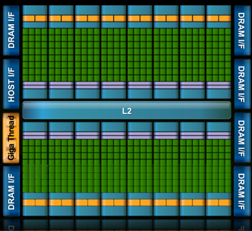
As a quick refresher, the GF100 is composed of 512 SPs, which NVIDIA now calls CUDA cores. Each CUDA core is organized in to a block of 32 cores which we call a Streaming Multiprocessor (SM), which in turn are laid out so that 4 of them are in a Graphics Processing Cluster (GPC). Finally, there are 4 GPCs in a single GF100 chip. 32x4x4 = 512 CUDA cores.
| GF100 | GT200x2 (GTX 295) | GT200 (GTX 285) | G92 (9800+ GTX) | |
| Stream Processors | 512 | 2 x 240 | 240 | 128 |
| Texture Address / Filtering | 64/256 | 2 x 80 / 80 | 80 / 80 | 64 / 64 |
| ROPs | 48 | 2x 28 | 32 | 16 |
| Core Clock | ? | 576MHz | 648MHz | 738MHz |
| Shader Clock | ? | 1242MHz | 1476MHz | 1836MHz |
| Memory Clock | ? GDDR5 | 999MHz (1998MHz data rate) GDDR3 | 1242MHz (2484MHz data rate) GDDR3 | 1100MHz (2200MHz data rate) GDDR3 |
| Memory Bus Width | 384-bit | 2 x 448-bit | 512-bit | 256-bit |
| Frame Buffer | ? | 2 x 896MB | 1GB | 512MB |
| Transistor Count | 3B | 2 x 1.4B | 1.4B | 754M |
| Manufacturing Process | TSMC 40nm | TSMC 55nm | TSMC 55nm | TSMC 55nm |
| Price Point | $? | $500 | $400 | $150 - 200 |
When NVIDIA first unveiled GF100, we did not know anything about the ROPs, texture units, or any of the fixed-function graphics units that are customary in a GPU. Today we now have that information, and can discuss where it goes.
While GF100 resembles GT200 in a number of ways as a compute GPU, as a gaming GPU it’s very close to being a complete departure from GT200. The big change here is that the single block of fixed-function hardware as we know it is gone. Virtually every piece of hardware has been split up and moved down a level, and can now be found as part of a GPC or as a SM. NVIDIA’s GF100 block diagram does a good job of showing this.

What’s left of the fixed function hardware is the GigaThread Engine, which is what NVIDIA is calling their scheduler. To understand where our fixed function hardware went, we must meet the newest execution units: The PolyMorph Engine and the Raster Engine.

We’ll start with the Raster Engine. The Raster Engine is the combination of all the raster related hardware that we would have found previously in the fixed function pipeline. It does edge/triangle setup, rasterization, and z-culling in a pipelined manner. Each GPC has its own Raster Engine. NVIDIA has very little to say about the Raster Engine, but very little has changed from GT200 besides the fact that there are now 4 of them (one for each GPC) as opposed to 1 larger block. Each rasterizer can do 8 pixels per clock, for a total of 32 pixels per clock over the entirety of GF100.
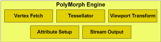
The much more important of the two new execution units is the PolyMorph Engine, which is what NVIDIA is calling the execution unit that handles geometry for GF100. The PolyMorph Engine is responsible for handling Vertex Fetch, Tessellation, Viewport Transform, Attribute Setup, and Stream Output. It’s here where the Tessellator is located, one of the biggest changes that DX11 is bringing to GPU design. Unlike the Raster Engine, each SM has a PolyMorph Engine, giving the GF100 16 PolyMorph Engines altogether.
While the PolyMoprh Engine may sound simple in its description, don’t let it fool you. NVIDIA didn’t just move their geometry hardware to a different place, clone it 15 times, and call it a day. This was previously fixed-function hardware where a single unit sat in a pipeline and did its share of the work. By splitting up the fixed-function pipeline like this, NVIDIA in actuality created a lot of work for themselves. Why? Out of order execution.
OoO is something we usually reserve for CPUs, where high-end CPUs are built to execute instructions out of order in order to extract more performance out of them through instruction level parallelism. OoO is very hard to accomplish, because you can only execute certain instructions ahead of other ones while maintaining the correct result for your data. Execute an add instruction that relies on a previous operation before that’s done, and you have problems. GF100 isn’t a full OoO design, so we’re not going to cover OoO in-depth here, but if you’d like to know more please see this article.
At any rate, internally each PolyMorph Engine is still a simple in-order design. NVIDIA hasn’t gone so far as to make a PolyMorph Engine an OoO design – but because there are 16 of them when there used to be just 1, OoO hazards can occur just as they would in an OoO executing CPU. NVIDIA now has to keep track of what each PolyMorph Engine is doing in respect to the other 15, and put the brakes on any of them that get too far ahead in order to maintain the integrity of results.
To resolve the hazards of OoO, GF100 has a private communication channel just for the PolyMorph Engines that allows them to stay together on a task in spite of being spread apart. The fact of the matter is that all of the work that goes in to making a design like this work correctly is an immense amount of effort, and NVIDIA’s engineers are quite proud of this effort. They have taken the monolithic design of prior GPUs’ geometry units, and made it parallel. We can’t overstate how much of an engineering challenge this is.
However all of this work came at a cost, and not just the significant engineering resources NVIDIA threw at GF100. The other cost was time – we believe that the PolyMorph Engine is the single biggest reason that GF100 didn’t make it out last year. It’s the single biggest redesign of any component in GF100, and is something that NVIDIA had to start virtually from scratch on. When NVIDIA told us that designing a big GPU is hard, this is what they had in mind.
Now why did NVIDIA put themselves through all of this? Because in their eyes, they had to. The use of a fixed-function pipeline in their eyes was a poor choice given the geometric complexity that a tessellator would create, and hence the entire pipeline needed to be rebalanced. By moving to the parallel design of the PolyMorph Engine, NVIDIA’s geometry hardware is no longer bound by any limits of the pipelined fixed-function design (such as bottlenecks in one stage of the pipeline), and for better or for worse, they can scale their geometry and raster abilities with the size of the chip. A smaller GF100 derivative will not have as many PolyMorph or Raster units as GF100, and as a result won’t have the same level of performance; G92 derivatives and AMD’s designs both maintain the same fixed function pipeline through all chips, always offering the same level of performance.

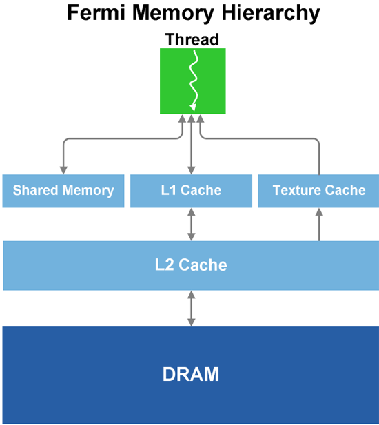
Speaking of performance, we’ll get to that in a bit, but for now we’ll finish our discussion of GF100’s graphics units. Each SM has 4 texture units, which have changes somewhat from the GT200. In GT200, the texture units were at the TPC level; here they are per SM. The texture units are also affected by the cache reorganization of GF100; for L1 cache they still have the same 12KB of texture cache per set of 4 texture units, while they all share GF100’s 768KB L2 cache, which is now used by all execution units and not just textures. Each unit can compute 1 texture address and fetch 4 texture samples per clock, a significantly higher texture fetch rate than on the GT200. Furthermore in conjunction with DX11, NVIDIA’s texture units now support DX11’s new compressed texture formats. Finally, texture units are now tied to the shader clock and not the core clock. They run at 1/2 the shader clock speed of GF100.
Last but not least, this brings us to the ROPs. The ROPs have been reorganized, there are now 48 of them in 6 parttions of 8, and a 64bit memory channel serving each partition. The ROPs now share the L2 cache with the rest of GF100, while under GT200 they had their own L2 cache. Each ROP can do 1 regular 32bit pixel per clock, 1 FP16 pixel over 2 clocks, or 1 FP32 pixel over 4 clocks, giving the GF100 the ability to retire 48 regular pixels per clock. The ROPs are clocked together with the L2 cache.
That leaves us on a final note: clocks. The core clock has been virtually done away with on GF100, as almost every unit now operates at or on a fraction of the shader clock. Only the ROPs and L2 cache operate on a different clock, which is best described as what’s left of the core clock. The shader clock now drives the majority of the chip, including the shaders, the texture units, and the new PolyMorph and Raster Engines. Specifically, the texture units, PolyMorph Engine, and Raster Engine all run at 1/2 shader clock (which NVIDIA is tentatively calling the "GPC Clock"), while the L1 cache and the shaders themselves run at the full shader clock. Don’t be surprised if GF100 overclocking is different from GT200 overclocking as a result.
Why NVIDIA Is Focused On Geometry
Up until now we haven’t talked a great deal about the performance of GF100, and to some extent we still can’t. We don’t know the final clock speeds of the shipping cards, so we don’t know exactly what the card will be like. But what we can talk about is why NVIDIA made the decisions they did: why they went for the parallel PolyMorph and Raster Engines.
The DX11 specification doesn’t leave NVIDIA with a ton of room to add new features. Without the capsbits, NVIDIA can’t put new features on their hardware and easily expose them, nor would they want to at risk of having those features (and hence die space) go unused. DX11 rigidly says what features a compliant video card should offer, and leaves you very little room to deviate.
So NVIDIA has taken a bit of a gamble. There’s no single wonder-feature in the hardware that immediately makes it stand out from AMD’s hardware – NVIDIA has post-rendering features such as 3D Vision or compute features such as PhysX, but when it comes to rendering they can only do what AMD does.
But the DX11 specification doesn’t say how quickly you have to do it.
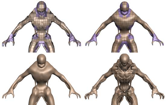
Tessellation in action
To differentiate themselves from AMD, NVIDIA is taking the tessellator and driving it for all its worth. While AMD merely has a tessellator, NVIDIA is counting on the tessellator in their PolyMorph Engine to give them a noticeable graphical advantage over AMD.
To put things in perspective, between NV30 (GeForce FX 5800) and GT200 (GeForce GTX 280), the geometry performance of NVIDIA’s hardware only increases roughly 3x in performance. Meanwhile the shader performance of their cards increased by over 150x. Compared just to GT200, GF100 has 8x the geometry performance of GT200, and NVIDIA tells us this is something they have measured in their labs.
So why does NVIDIA want so much geometry performance? Because with tessellation, it allows them to take the same assets from the same games as AMD and generate something that will look better. With more geometry power, NVIDIA can use tessellation and displacement mapping to generate more complex characters, objects, and scenery than AMD can at the same level of performance. And this is why NVIDIA has 16 PolyMorph Engines and 4 Raster Engines, because they need a lot of hardware to generate and process that much geometry.
NVIDIA believes their strategy will work, and if geometry performance is as good as they say it is, then we can see why they feel this way. Game art is usually created at far higher levels of detail than what eventually ends up being shipped, and with tessellation there’s no reason why a tessellated and displacement mapped representation of that high quality art can’t come with the game. Developers can use tessellation to scale down to whatever the hardware can do, and in NVIDIA’s world they won’t have to scale it down very far to meet up with the GF100.
At this point tessellation is a message that’s much more for developers than it is consumers. As DX11 is required to take advantage of tessellation, only a few games exist while plenty more are on the way. NVIDIA needs to convince developers to ship their art with detailed enough displacement maps to match GF100’s capabilities, and while that isn’t too hard, it’s also not a walk in the park. To that extent they’re also extolling the other virtues of tessellation, such as the ability to do higher quality animations by only needing to animate the control points of a model, and letting tessellation take care of the rest. A lot of the success of the GF100 architecture is going to ride on how developers respond to this, so it’s going to be something worth keeping an eye on.
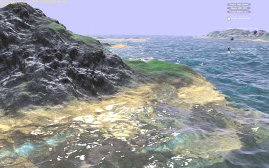
NVIDIA's water tessellation demo
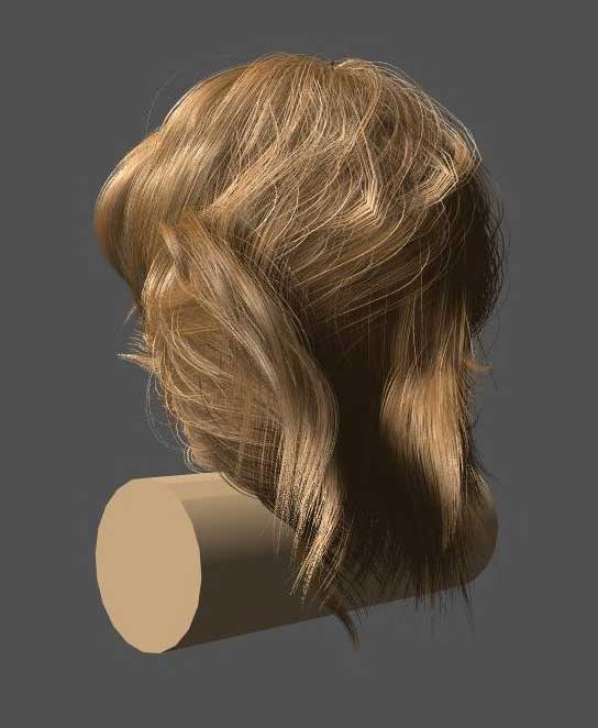
NVIDIA's hair tessellation demo
Better Image Quality: Jittered Sampling & Faster Anti-Aliasing
As we’ve stated before, the DX11 specification generally leaves NVIDIA’s hands tied. Without capsbits they can’t easily expose additional hardware features beyond what DX11 calls for, and even if they could there’s always the risk of building hardware that almost never gets used, such as AMD’s Tessellator on the 2000-4000 series.
So the bulk of the innovation has to come from something other than offering non-DX11 functionality to developers, and that starts with image quality.
We bring up DX11 here because while it strongly defines what features need to be offered, it says very little about how things work in the backend. The Polymorph Engine is of course one example of this, but there is another case where NVIDIA has done something interesting on the backend: jittered sampling.
Jittered sampling is a long-standing technique used in shadow mapping and various post-processing techniques. In this case, jittered sampling is usually used to create soft shadows from a shadow map – take a random sample of neighboring texels, and from that you can compute a softer shadow edge. The biggest problem with jittered sampling is that it’s computationally expensive and hence its use is limited to where there is enough performance to pay for it.
In DX10.1 and beyond, jittered sampling can be achieved via the Gather4 instruction, which as the name implies is the instruction that gathers the neighboring texels for jittered sampling. Since DX does not specify how this is implemented, NVIDIA implemented it in hardware as a single vector instruction. The alternative is to fetch each texel separately, which is how this would be manually implemented under DX10 and DX9.
NVIDIA’s own benchmarks put the performance advantage of this at roughly 2x over the non-vectorized implementation on the same hardware. The benefit for developers will be that those who implement jittered sampling (or any other technique that can use Gather4) will find it to be a much less expensive technique here than it was on NVIDIA’s previous generation hardware. For gamers, this will mean better image quality through the greater use of jittered sampling.
Meanwhile anti-aliasing performance overall received a significant speed boost. As with AMD, NVIDIA has gone ahead and tweaked their ROPs to reduce the performance hit of 8x MSAA, which on previous-generation GPUs could result in a massive performance drop. In this case NVIDIA has improved the compression efficiency in the ROPs to reduce the hit of 8x MSAA, and also cites the fact that having additional ROPs improves performance by allowing the hardware to better digest smaller primitives that can’t compress well.
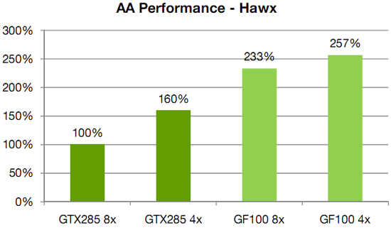
NVIDIA's HAWX data - not independently verified
This is something we’re certainly going to be testing once we have the hardware, although we’re still not sold on the idea that the quality improvement from 8x MSAA is worth any performance hit in most situations. There is one situation however where additional MSAA samples do make a stark difference, which we’ll get to next.
Better Image Quality: CSAA & TMAA
NVIDIA’s next big trick for image quality is that they’ve revised Coverage Sample Anti-Aliasing. CSAA, which was originally introduced with the G80, is a lightweight method of better determining how much of a polygon actually covers a pixel. By merely testing polygon coverage and storing the results, the ROP can get more information without the expense of fetching and storing additional color and Z data as done with a regular sample under MSAA. The quality improvement isn’t as pronounced as just using more multisamples, but coverage samples are much, much cheaper.
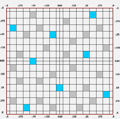
32x CSAA sampling pattern
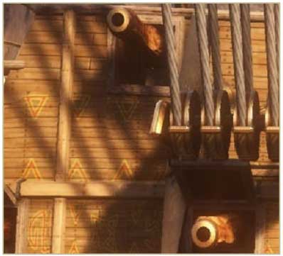
For the G80 and GT200, CSAA could only test polygon edges. That’s great for resolving aliasing at polygon edges, but it doesn’t solve other kinds of aliasing. In particular, GF100 will be waging a war on billboards – flat geometry that uses textures with transparency to simulate what would otherwise require complex geometry. Fences, leaves, and patches of grass in fields are three very common uses of billboards, as they are “minor” visual effects that would be very expensive to do with real geometry, and would benefit little from the quality improvement.
Since billboards are faking geometry, regular MSAA techniques do not remove the aliasing within the billboard. To resolve that DX10 introduced alpha to coverage functionality, which allows MSAA to anti-alias the fake geometry by using the alpha mask as a coverage mask for the MSAA process. The end result of this process is that the GPU creates varying levels of transparency around the fake geometry, so that it blends better with its surroundings.
It’s a great technique, but it wasn’t done all that well by the G80 and GT200. In order to determine the level of transparency to use on an alpha to coverage sampled pixel, the anti-aliasing hardware on those GPUs used MSAA samples to test the coverage. With up to 8 samples (8xQ MSAA mode), the hardware could only compute 9 levels of transparency, which isn’t nearly enough to establish a smooth gradient. The result was that while alpha to coverage testing allowed for some anti-aliasing of billboards, the result wasn’t great. The only way to achieve really good results was to use super-sampling on billboards through Transparency Super-Sample Anti-Aliasing, which was ridiculously expensive given that when billboards are used, they usually cover most of the screen.
For GF100, NVIDIA has made two tweaks to CSAA. First, additional CSAA modes have been unlocked – GF100 can do up to 24 coverage samples per pixel as opposed 16. The second change is that the CSAA hardware can now participate in alpha to coverage testing, a natural extension of CSAA’s coverage testing capabilities. With this ability CSAA can test the coverage of the fake geometry in a billboard along with MSAA samples, allowing the anti-aliasing hardware to fetch up to 32 samples per pixel. This gives the hardware the ability to compute 33 levels of transparency, which while not perfect allows for much smoother gradients.
The example NVIDIA has given us for this is a pair of screenshots taken from a field in Age of Conan, a DX10 game. The first screenshot is from a GT200 based video card running the game with NVIDIA’s 16xQ anti-aliasing mode, which is composed of 8 MSAA samples and 8 CSAA samples. Since the GT200 can’t do alpha to coverage testing using the CSAA samples, the resulting grass blades are only blended with 9 levels of transparency based on the 8 MSAA samples, giving them a dithered look.
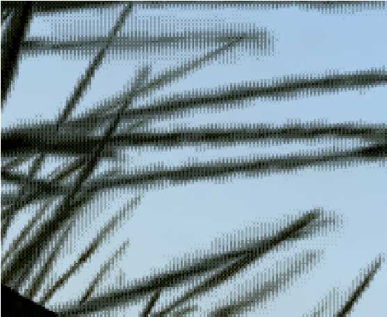
Age of Conan grass, GT200 16x AA
The second screenshot is from GF100 running in NVIDIA’s new 32x anti-aliasing mode, which is composed of 8 MSAA samples and 24 CSAA samples. Here the CSAA and MSAA samples can be used in alpha to coverage, giving the hardware 32 samples from which to compute 33 levels of transparency. The result is that the blades of grass are still somewhat banded, but overall much smoother than what the GT200 produced. Bear in mind that since 8x MSAA is faster on the GF100 than it was GT200, and CSAA has very little overhead in comparison (NVIDIA estimates 32x has 93% of the performance of 8xQ), the entire process should be faster on GF100 even if it were running at the same speeds as GT200. Image quality improved, and at the same time the performance improved too.

Age of Conan grass, GF100 32x AA
The ability to use CSAA on billboards left us with a question however: isn’t this what Transparency Anti-Aliasing was for? The answer as it turns out is both yes and no.
Transparency Anti-Aliasing was introduced on the G70 (GeForce 7800GTX) and was intended to help remove aliasing on billboards, exactly what NVIDIA is doing today with MSAA. The difference is that while DX10 has alpha to coverage, DX9 does not – and DX9 was all there was when G70 was released. Transparency Multi-Sample Anti-Aliasing (TMAA) as implemented today is effectively a shader replacement routine to make up for what DX9 lacks. With it, DX9 games can have alpha to coverage testing done on their billboards in spite of DX9 not having this feature, allowing for image quality improvements on games still using DX9. Under DX10 TMAA is superseded by alpha to coverage in the API, but TMAA is still alive and well due to the large number of older games using DX9 and the large number of games yet to come that will still use DX9.
Because TMAA is functionally just enabling alpha to coverage on DX9 games, all of the changes we just mentioned to the CSAA hardware filter down to TMAA. This is excellent news, as TMAA has delivered lackluster results in the past – it was better than nothing, but only Transparency Super-Sample Anti-Aliasing (TSAA) really fixed billboard aliasing, and only at a high cost. Ultimately this means that a number of cases in the past where only TSAA was suitable are suddenly opened up to using the much faster TMAA, in essence making good billboard anti-aliasing finally affordable on newer DX9 games on NVIDIA hardware.
As a consequence of this change, TMAA’s tendency to have fake geometry on billboards pop in and out of existence is also solved. Here we have a set of screenshots from Left 4 Dead 2 showcasing this in action. The GF100 with TMAA generates softer edges on the vertical bars in this picture, which is what stops the popping from the GT200.
Left 4 Dead 2: TMAA on GT200
Left 4 Dead 2: TMAA on GF100
Applications of GF100’s Compute Hardware
Last but certainly not least are the changes to gaming afforded by the improved compute/shader hardware. NVIDIA believes that by announcing the compute abilities so far ahead of the gaming abilities of the GF100, that potential customers have gotten the wrong idea about NVIDIA’s direction. Certainly they’re increasing their focus on the GPGPU market, but as they’re trying their hardest to point out, most of that compute hardware has a use in gaming too.
Much of this is straightforward: all of the compute hardware is what processes the pixel and vertex shader commands, so the additional CUDA cores in the GF100 give it much more shader power than the GT200. We also have DirectCompute, which can use the compute hardware to quickly do some things that couldn’t be done quickly via shader code, such as Self Shadowing Ambient Occlusion in games like Battleforge, or to take an NVIDIA example, the depth-of-field effect in Metro 2033.
Perhaps the single biggest improvement for gaming that comes from NVIDIA’s changes to the compute hardware are the benefits afforded to compute-like tasks for gaming. PhysX plays a big part here, as along with DirectCompute it’s going to be one of the biggest uses of compute abilities when it comes to gaming.
NVIDIA is heavily promoting the idea that GF100’s concurrent kernels and fast context switching abilities are going to be of significant benefit here. With concurrent kernels, different PhysX simulations can start without waiting for other SMs to complete the previous simulation. With fast context switching, the GPU can switch from rendering to PhysX and back again while wasting less time on the context switch itself. The result is that there’s going to be less overhead in using the compute abilities of GF100 during gaming, be it for PhysX, Bullet Physics, or DirectCompute.
NVIDIA is big on pushing specific examples here in order to entice developers in to using these abilities, and a number of demo programs will be released along with GF100 cards to showcase these abilities. Most interesting among these is a ray tracing demo that NVIDIA is showing off. Ray tracing is something even G80 could do (albeit slowly) but we find this an interesting way for NVIDIA to go since promoting ray tracing puts them in direct competition with Intel, who has been showing off ray tracing demos running on CPUs for years. Ray tracing nullifies NVIDIA’s experience in rasterization, so to promote its use is one of the riskier things they can do in the long-term.

NVIDIA's car ray tracing demo
At any rate, the demo program they are showing off is a hybrid program that showcases the use of both rasterization and ray tracing for rendering a car. As we already know from the original Fermi introduction, GF100 is supposed to be much faster than GT200 at ray tracing, thanks in large part due to the L1 cache architecture of GF100. The demo we saw of a GF100 card next to a GT200 card had the GF100 card performing roughly 3x as well as the GT200 card. This specific demo still runs at less than a frame per second (0.63 on the GF100 card) so it’s by no means true real-time ray tracing, but it’s getting faster all the time. For lower quality ray tracing, certainly this would be doable in real-time.
Dark Void's turbulence in action
NVIDIA is also showing off several other demos of compute for gaming, including a PhysX fluid simulation, the new PhysX APEX turbulence effect on Dark Void, and an AI path finding simulation that we did not have a chance to see. Ultimately PhysX is still NVIDIA’s bigger carrot for consumers, while the rest of this is to entice developers to make use of the compute hardware through whatever means they’d like (PhysX, OpenCL, DirectCompute). Outside of PhysX, heavy use of the GPU compute abilities is still going to be some time off.
3D Vision Surround: NVIDIA’s Eyefinity
During our meeting with NVIDIA, they were also showing off 3D Vision Surround, which was announced at the start of CES at their press conference. 3D Vision Surround is not inherently a GF100 technology, but since it’s being timed for release along-side GF100 cards, we’re going to take a moment to discuss it.
If you’ve seen Matrox’s TripleHead2Go or AMD’s Eyefinity in action, then you know what 3D Vision Surround is. It’s NVIDIA’s implementation of the single large surface concept so that games (and anything else for that matter) can span multiple monitors. With it, gamers can get a more immersive view by being able to surround themselves with monitors so that the game world is projected from more than just a single point in front of them.
NVIDIA tells us that they’ve been sitting on this technology for quite some time but never saw a market for it. With the release of TripleHead2Go and Eyefinity it became apparent to them that this was no longer the case, and they unboxed the technology. Whether this is true or a sudden reaction to Eyefinity is immaterial at the moment, as it’s coming regardless.
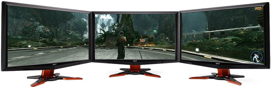
This triple-display technology will have two names. When it’s used on its own, NVIDIA is calling it NVIDIA Surround. When it’s used in conjunction with 3D Vision, it’s called 3D Vision Surround. Obviously NVIDIA would like you to use it with 3D Vision to get the full effect (and to require a more powerful GPU) but 3D Vision is by no means required to use it. It is however the key differentiator from AMD, at least until AMD’s own 3D efforts get off the ground.
Regardless of to what degree this is a sudden reaction from NVIDIA over Eyefinity, ultimately this is something that was added late in to the design process. Unlike AMD who designed the Evergreen family around it from the start, NVIDA did not, and as a result they did not give a GF100 the ability to drive more than 2 displays at once. The shipping GF100 cards will have the traditional 2 monitor limit, meaning that gamers will need 2 GF100 cards in SLI to drive 3+ monitors, with the second card needed to provide the 3rd and 4th display outputs. We expect that the next NVIDIA design will include the ability to drive 3+ monitors from a single GPU, as for the moment this limitation precludes any ability to do Surround for cheap.
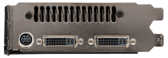
GTX 280 with 2 display outputs: GF100 won't be any different
As for some good news, as we stated earlier this is not a technology inherent to the GF100. NVIDIA can do it entirely in software and as a result will be backporting this technology to the GT200 (GTX 200 series). The drivers that get released for the GF100 will allow GTX 200 cards to do Surround in the same manner: with 2 cards, you can run a single large surface across 3+ displays. We’ve seen this in action and it works, as NVIDIA was demoing a pair of GTX 285s running in NVIDIA Surround mode in their CES booth.
The big question of course is going to be what this does for performance on both the GF100 and GT200, along with compatibility. That’s something that we’re going to have to wait on the actual hardware for.
Final Words
On a final note, we’ll end with a quick look at Supersonic Sled, NVIDIA’s big “kitchen sink” demo for GF100. Supersonic Sled is a comically-themed simulation of a sled with a rocket attached (or perhaps the other way around) based on some real 1950’s US Air Force tests. It uses tessellation, DirectCompute, PhysX – every new thing NVIDIA could throw in to a demo and still have it run. We had a chance to see this in action on a 3D Vision Surround setup at CES, and we have to give NVIDIA’s demo team credit here, they rarely disappoint.

NVIDIA did give us a small (7MB) recording of it in action that we’ve posted here, in case you haven’t had a chance to see any of the recordings from the CES showfloor.
With that out of the way, there’s only so much we can say about NVIDIA’s new architecture without having the hardware on-hand for testing. NVIDIA certainly built a GPU compute monster in GF100, and based on what we now know about its graphics abilities, it looks like it’s an equally capable GPU gaming monster.
But the big question is just how much of a monster will it be, and what kind of monster price tag will it come with? Let’s make no mistake, at 3 billion transistors GF100 is going to be big, and from NVIDIA’s hints it’s probably going to be the single hottest single-GPU card we’ve seen yet. Barring any glaring flaws NVIDIA has what looks to be a solid design, but at the end of the day it almost always boils down to “how fast?” and “how much?”
![]()
NVIDIA has taken a big risk on GF100, first with its compute abilities for GPGPU use, then on its geometry abilities for gaming, and now the risk is time. Being 6 months late has hurt NVIDIA, and being 6 months late has hurt consumers through uncompetitive pricing from AMD. By no means is the situation dire, but we can quickly come up with some scenarios where it is if NVIDIA can’t convincingly beat AMD in gaming performance.
NVIDIA has shown their cards, and they’re all in. Now in the next couple of months we’ll see if they’re bluffing or if they really have what it takes to win. Stay tuned.


