Understanding Camera Optics & Smartphone Camera Trends, A Presentation by Brian Klug
by Brian Klug on February 22, 2013 5:04 PM EST- Posted in
- Smartphones
- camera
- Android
- Mobile
The Camera Module & CMOS Sensor Trends
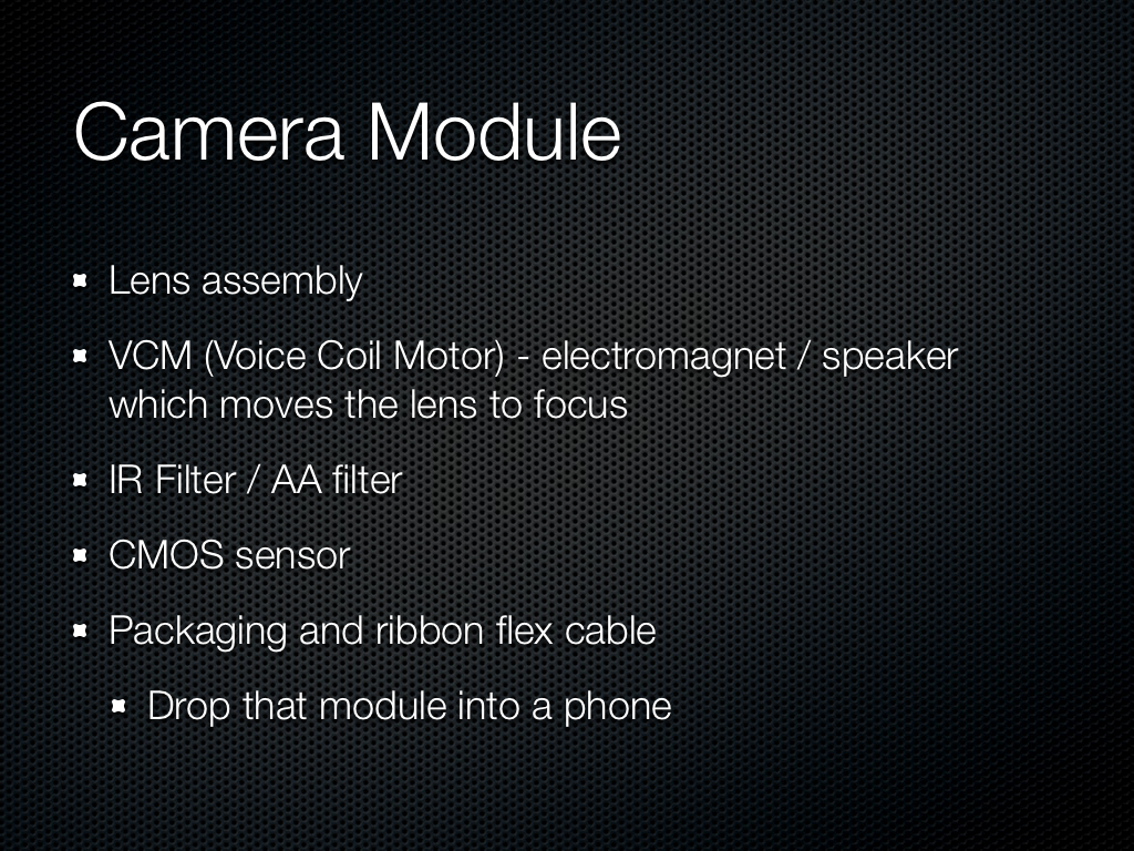
So after we have the lenses, what does that go into? Turns out there is some standardization, and that standardization for packaging is called a module. The module consists of of course our lens system, an IR filter, voice coil motor for focusing, and finally the CMOS and fanout ribbon cable. Fancy systems with OIS will contain a more complicated VCM and also a MEMS gyro somewhere in the module.

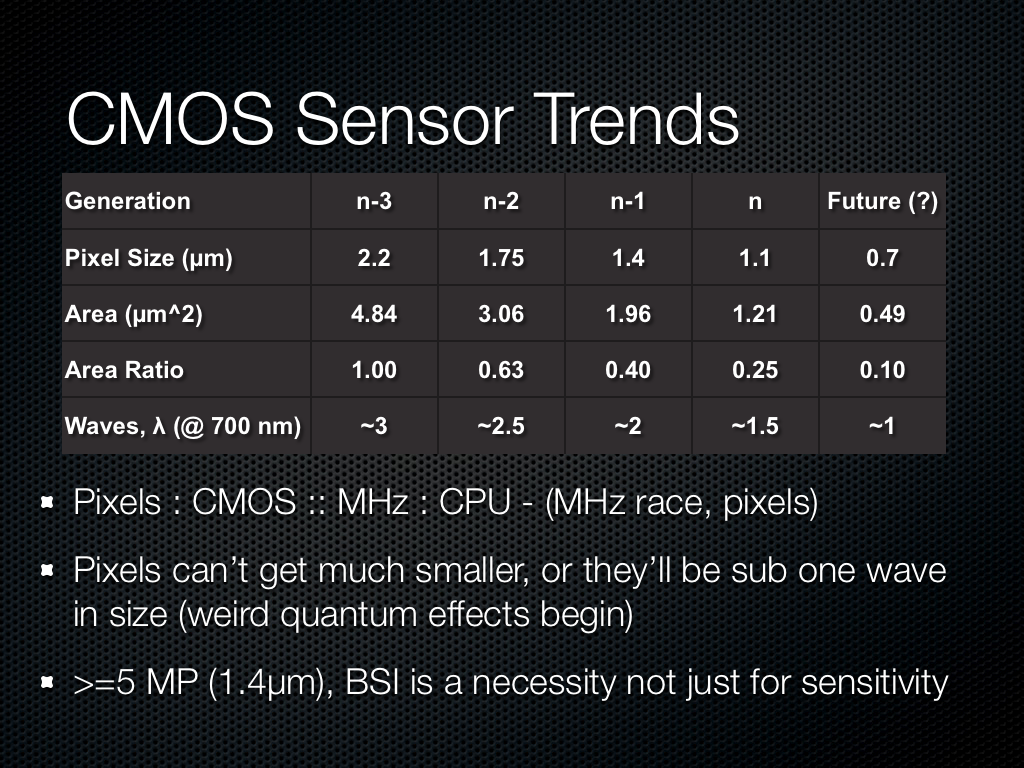
Onto CMOS, which is of course the image sensor itself. Most smartphone CMOSes end up being between 1/4“ and 1/3” in optical format, which is pretty small. There are some outliers for sure, but at the high end this is by far the prevailing trend. Optical format is again something we need to go look at a table for or consult the manufacturer about. Front facing sensors are way smaller, unsurprisingly. The size of the CMOS in most smartphones has been relatively fixed because going to a larger sensor would necessitate a thicker optical system, thus the real trend to increase megapixels has been more of smaller pixels.

The trend in pixel size has been pretty easy to follow, with each generation going to a different size pixel to drive megapixel counts up. The current generation of modern pixels is around 1.1 microns square, basically any 13 MP smartphone is shipping 1.1 microns, like the Optimus G, and interestingly enough others are using 1.1 microns at 8 MP to drive thinner modules, like the thinner Optimus G option or Nexus 4. The previous generation of 8 MP sensors were using 1.4 micron pixels, and before that at 5 MP we were talking 1.65 or 1.75 micron pixels. Those are pretty tiny pixels, and if you stop and think about a wave of very red light at around 700nm, we’re talking about 1.5 waves with 1.1 micron pixels, around 2 waves at 1.4 microns, and so forth. There’s really not much smaller you can go, it doesn’t make sense to go smaller than one wave.
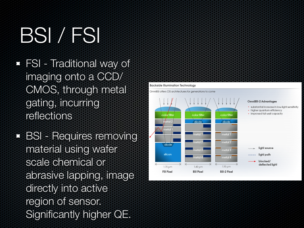
There was a lot of talk about the difference between backside (BSI) and front side illumination (FSI) for systems as well. BSI images directly through silicon into the active region of the pixel, whereas FSI images through metal layers which incur reflections and a smaller area and thus loss of light. BSI has been around for a while in the industrial and scientific field for applications wanting the highest quantum efficiency (conversion of photons to electrons), and while they were adopted in smartphone use to increase the sensitivity (quantum efficiency) of these pixels, there’s an even more important reason. With pixels this small in 2D profile (eg 1.4 x 1.4 microns) the actual geometry of a pixel began to look something like a long hallway, or very tall cylinder. The result would be quantum blur where a photon being imaged onto the surface of the pixel, converted to an electron, might not necessarily map to the appropriate active region underneath - it takes an almost random walk for some distance. In addition the numerical aperture of these pixels wouldn’t be nearly good enough for the systems they would be paired with.
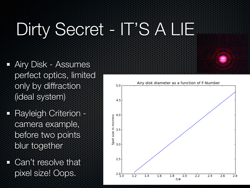
Around the time I received the One X and One S last year, I finally became curious about whether we could ever see nice bokeh (blurry background) with an F/2.0 system and small pixels. While trapped on some flight somewhere, I finally got bored enough to go quantify what this would be, and a side effect of this was some question about whether an ideal, diffraction limited (no aberrations, ideal, if we had perfect optics) system could even resolve a spot the size of the pixels on these sensors.

It turns out that we can’t, really. If we look at the airy disk diameter formed from a perfect diffraction limited HTC One X or S camera system (the parameters I chose since at the time this was, and still is, the best system on paper), we get a spot size around 3.0 microns. There’s some fudge factor here since interpolation takes place thanks to there being a bayer grid atop the CMOS that then is demosaiced, more on that later, so we’re close to being at around the right size, but obviously 1.1 microns is just oversampling.
Oh, and also here are some hyperfocal distance plots as a function of pixel size and F/# for the same system. It turns out that everything is in focus pretty close to your average smartphone, so you have to be petty close to the subject to get a nice bokeh effect.


60 Comments
View All Comments
Sea Shadow - Friday, February 22, 2013 - link
I am still trying to digest all of the information in this article, and I love it!It is because of articles like this that I check Anandtech multiple times per day. Thank you for continuing to provide such insightful and detailed articles. In a day and age where other "tech" sites are regurgitating the same press releases, it is nice to see anandtech continues to post detailed and informative pieces.
Thank you!
arsena1 - Friday, February 22, 2013 - link
Yep, exactly this.Thanks Brian, AT rocks.
ratte - Friday, February 22, 2013 - link
Yeah, got to echo the posts above, great article.vol7ron - Wednesday, February 27, 2013 - link
Optics are certainly an area the average consumer knows little about, myself included.For some reason it seems like consumers look at a camera's MP like how they used to view a processor's Hz; as if the higher number equates to a better quality, or more efficient device - that's why we can appreciate articles like these, which clarify and inform.
The more the average consumer understands, the more they can demand better products from manufacturers and make better educated decisions. In addition to being an interesting read!
tvdang7 - Friday, February 22, 2013 - link
Same here they have THE BEST detail in every article.Wolfpup - Wednesday, March 6, 2013 - link
Yeah, I just love in depth stuff like this! May end up beyond my capabilities but none the less I love it, and love that Brian is so passionate about it. It's so great to hear on the podcast when he's ranting about terrible cameras! And I mean that, I'm not making fun, I think it's awesome.Guspaz - Friday, February 22, 2013 - link
Is there any feasibility (anything on the horizon) to directly measure the wavelength of light hitting a sensor element, rather than relying on filters? Or perhaps to use a layer on top of the sensor to split the light rather than filter the light? You would think that would give a substantial boost in light sensitivity, since a colour filter based system by necessity blocks most of the light that enters your optical system, much in the way that 3LCD projector produces a substantially brighter image than a single-chip DLP projector given the same lightbulb, because one splits the white light and the other filters the white light.HibyPrime1 - Friday, February 22, 2013 - link
I'm not an expert on the subject so take what I'm saying here with a grain of salt.As I understand it you would have to make sure that no more than one photon is hitting the pixel at any given time, and then you can measure the energy (basically energy = wavelength) of that photon. I would imagine if multiple photons are hitting the sensor at the same time, you wouldn't be able to distinguish how much energy came from each photon.
Since we're dealing with single photons, weird quantum stuff might come into play. Even if you could manage to get a single photon to hit each pixel, there may be an effect where the photons will hit multiple pixels at the same time, so measuring the energy at one pixel will give you a number that includes the energy from some of the other photons. (I'm inferring this idea from the double-slit experiment.)
I think the only way this would be possible is if only one photon hits the entire sensor at any given time, then you would be able to work out it's colour. Of course, that wouldn't be very useful as a camera.
DominicG - Saturday, February 23, 2013 - link
Hi Hlbyphotodetection does not quite work like that. A photon hitting a photodiode junction either has enough energy to excite an electron across the junction or it does not. So one way you could make a multi-colour pixel would be to have several photodiode junctions one on top of the other, each with a different "energy gap", so that each one responds to a different wavelength. This idea is now being used in the highest efficiency solar cells to allow all the different wavelengths in sunlight to be absorbed efficiently. However for a colour-sensitive photodiode, there are some big complexities to be overcome - I have no idea if anyone has succeeded or even tried.
HibyPrime1 - Saturday, February 23, 2013 - link
Interesting. I've read about band-gaps/energy gaps before, but never understood what they mean in any real-world sense. Thanks for that :)