The Haswell Review: Intel Core i7-4770K & i5-4670K Tested
by Anand Lal Shimpi on June 1, 2013 10:00 AM ESTDie Size and Transistor Count
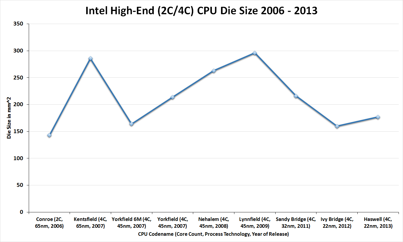
Moving on to die sizes and transistor counts, this year Intel is striving to be more straightforward and accurate than was the case with Sandy Bridge and Ivy Bridge. With the Bridge generation we didn’t initially get comparable numbers, only for the correction to throw in additional confusion. For Haswell Intel is laying things out from the start, listing both possible numbers so that either can be compared.
| CPU Specification Comparison | |||||||||
| CPU | Manufacturing Process | Cores | GPU | Transistor Count (Schematic) | Die Size | ||||
| Haswell GT3 4C | 22nm | 4 | GT3 | ? | 264mm2 (est) | ||||
| Haswell GT2 4C | 22nm | 4 | GT2 | 1.4B | 177mm2 | ||||
| Haswell ULT GT3 2C | 22nm | 2 | GT3 | 1.3B | 181mm2 | ||||
| Intel Ivy Bridge 4C | 22nm | 4 | GT2 | 1.2B | 160mm2 | ||||
| Intel Sandy Bridge E 6C | 32nm | 6 | N/A | 2.27B | 435mm2 | ||||
| Intel Sandy Bridge 4C | 32nm | 4 | GT2 | 995M | 216mm2 | ||||
| Intel Lynnfield 4C | 45nm | 4 | N/A | 774M | 296mm2 | ||||
| AMD Trinity 4C | 32nm | 4 | 7660D | 1.303B | 246mm2 | ||||
| AMD Vishera 8C | 32nm | 8 | N/A | 1.2B | 315mm2 | ||||
The two numbers for the most common Haswell configuration, Haswell GT2 4C, are 1.4 billion schematic transistors and 1.6 billion layout transistors. Why and what is the difference? The former count is the number of transistors in the schematic (hence the name), and is generally the number we go by when quoting transistor counts. Meanwhile the second number, the layout number, is the number of transistors used in the fabrication process itself. The difference comes from the fact that while the schematic will use one large transistor – being a logical diagram – production will actually use multiple transistors laid out in parallel for layout and process reasons. So how many transistors does Haswell have? It has both 1.4B and 1.6B, depending on which number we’re after, with 1.4B being the number Intel is passing around.
In any case, even among quad cores Haswell is going to come in a couple of different sizes. Along with the 1.4B transistor, 177mm2 4C/GT2 version of Haswell, there is the 4C/GT3 version of Haswell, which Intel doesn’t list the die size or transistor count for. Based on our rough measurements of the physical die we’re at 264mm2, which including the epoxy covering the die will run a bit large.
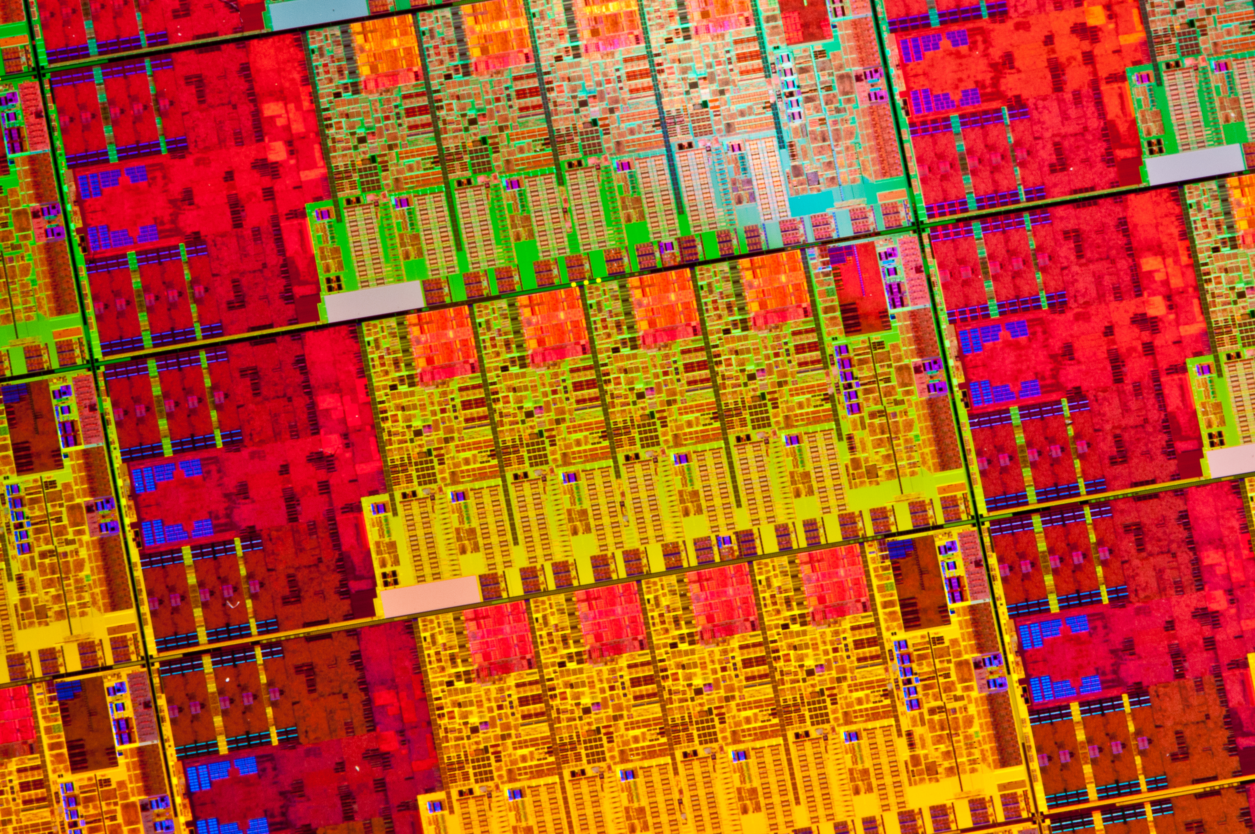
Breaking things down to the GPU portion of Haswell, based in turn on these measurements I came up with an 87mm^2 adder for the extra hardware in Haswell GT3 vs. GT2. Doubling that 87mm^2 we get a rough idea of how big the full 40 EU Haswell GPU might be: 174mm^2. If my math is right, this means that in a quad-core Haswell GT3 die, around 65% of the die area is GPU. This is contrary to the ~33% in a quad-core Haswell GT2. I suspect a dual-core + GT3 design is at least half GPU. Meanwhile Crystalwell, the 128MB eDRAM, adds another 84mm2 die (by our measurements) to the entire package.
On a comparative basis, the 4C/GT2 version of Haswell is roughly 200M transistors and 17mm2 bigger than the comparable 4C/GT2 version of Ivy Bridge. The transistor count increase is roughly what we’d expect, with most of those transistors going to Haswell itself while the GPU remains relatively unchanged. Though it’s interesting to note that while this marks a 17% increase in transistors, it’s only an 11% increase in die size. Ivy Bridge was a small die for an Intel, and while Haswell grows larger in exchange for the additional functionality the new architecture provides, it’s still a fairly small GPU and reaches a density greater than Ivy Bridge itself. Or to put this another way, Intel’s last tock CPU, Sandy Bridge, was larger still by almost 40mm2. It’s only once we start adding the relatively big GT3 GPU, and not the CPU, that we see Intel go well above 200mm2.


210 Comments
View All Comments
gregounech - Saturday, June 1, 2013 - link
Finally, let's see how good Haswell is.Krysto - Saturday, June 1, 2013 - link
Disappointing, to say the least. He's even comparing it to 2-3 older generations, just to be able to write some non-embarrassing numbers in the review, considering Haswell is only like 5-10% faster than IVB.The only big improvement seems to be in idle power consumption, of about 30%, which seems to "impress" Anand, but it just means that if your laptop had a 12h idle time, now it gets 16h.
It won't do much in ACTIVE power, which is really what matters. So much for all the "Haswell will totally dominate tablets in the near future" hype from Anand. Yes, this is not the mobile version, if Haswell really were an impressive design for power consumption, you'd see it here, too. It actually consumes 5-10% more than same clock speed IVB chip, which means its extra performance is almost completely negated.
This means that my predictions that Intel will try to "trick" us into thinking Haswell is ready for tablets will soon come true. Because if Haswell is not that efficient to warrant being used in "normal" tablets, then they'll try to dramatically lower clock speed and performance to even achieve 10W TDP (still too high for a tablet).
gregounech - Saturday, June 1, 2013 - link
Pretty good points.I'll still upgrade from my i5 750, and we won't get anything interesting until Skylake on the desktop (apparently, it wont be BGA), as I'm expecting motherboard OEMs to force us into buying their high end motherboards with any of the high end i7s Broadwell.
Samus - Sunday, June 2, 2013 - link
I'm using an i7-950 (over 4 years old) and its funny seeing how still-competitive it is to Intel's newest chips. It seems Sandy Bridge brought the bang and its just been trickle down performance since...Deelron - Sunday, June 2, 2013 - link
No kidding, I'm in the same boat and was thinking of upgrading but with my moderate over clock and these results have no problem waiting until the next generation.klmccaughey - Monday, June 3, 2013 - link
I'm still running my i5-2500k @ 4.3GHz and see nothing here of interest. I don't see myself upgrading any time soon.Hrel - Monday, June 3, 2013 - link
I'm still running an E8400. I see plenty of reason to upgrade.dananski - Monday, June 3, 2013 - link
Ahh I had one of those until this time last year. The E8400 found a happy home with a friend and I went to Ivy Bridge. Even small improvements like Sandy -> Ivy -> Haswell are useful, so don't feel too bad for having waited so long.vol7ron - Tuesday, June 4, 2013 - link
haha. I'm still running an OC'd E6600 (amongst others) for my desktop, which I hardly touch anymore, and am unsure whether to upgrade. I'm curious to see how Haswell performance vs power consumption vs price, is for NAS systems.Aside from natural degradation in one of the components (cpu, memory, psu, or gpu), which brings on an error every once in a while, the E6600 still does 98% of what I want of it and 100% of what I need it to do. So I suppose my needs are to get my electric bill down.
I need to read more because I was hoping this chip would bring me to buy a Surface Pro.
slickr - Wednesday, June 5, 2013 - link
You will get benefits upgrading from E6600 no doubt about it. For you its worth it as you are going to get a lot less power consumption, cooler operating chip and less noisy as well, with a significant performance increase especially in multithreaded applications, but for those thinking upgrading from Sandy or Ivy bridge to Haswell its worthless.I mean upgrading from 2500k to the new 4770k is useless. At best you are going to see 40% performance improvement which calculates into 5 seconds faster decoding or 5 seconds faster unzipping, but at worst you are going to get 2% performance increase which amounts to milliseconds of faster decoding and stuff.
You are not going to get less power consumption and it seems you may even get worse power consumption at loads. The new chips don't even overclock as well either, so its a waste of money to upgrade. If you have 3-4 generations older chip its worth upgrading, but else your money is better spent elsewhere.