NVIDIA Tegra K1 Preview & Architecture Analysis
by Brian Klug & Anand Lal Shimpi on January 6, 2014 6:31 AM ESTThe GPU
Despite the Denver surprise, the big story behind Tegra K1 is its GPU. Prior to K1, all previous Tegra designs implemented some derivative of what became known as the GeForce ULP core. This was a non-unified architecture that, at times, looked a lot like NV40. The design was never all that impressive from a performance or power efficiency standpoint. It was cost effective and often constrained by a narrow memory interface.
Going into Project Logan, which became Tegra K1, NVIDIA made the decision (around 3 years ago) to abandon the GeForce ULP roadmap and instead combine mobile and PC GPU roadmaps. Tegra K1 would be the first design to leverage a PC GPU, in this case Kepler. The bigger implication is that all future Tegra SoCs will integrate PC GPUs. The even crazier part of all of this is that all future NVIDIA GPUs will start out as mobile first designs (including Maxwell). Productization and market availability may happen in a different order, but all architectures will start as mobile designs and then be adopted to fit other, higher power segments. This is very much like Intel’s mobile-first realization of the mid-2000s with regards to notebook processors, but with NVIDIA and smartphone/tablet GPUs.
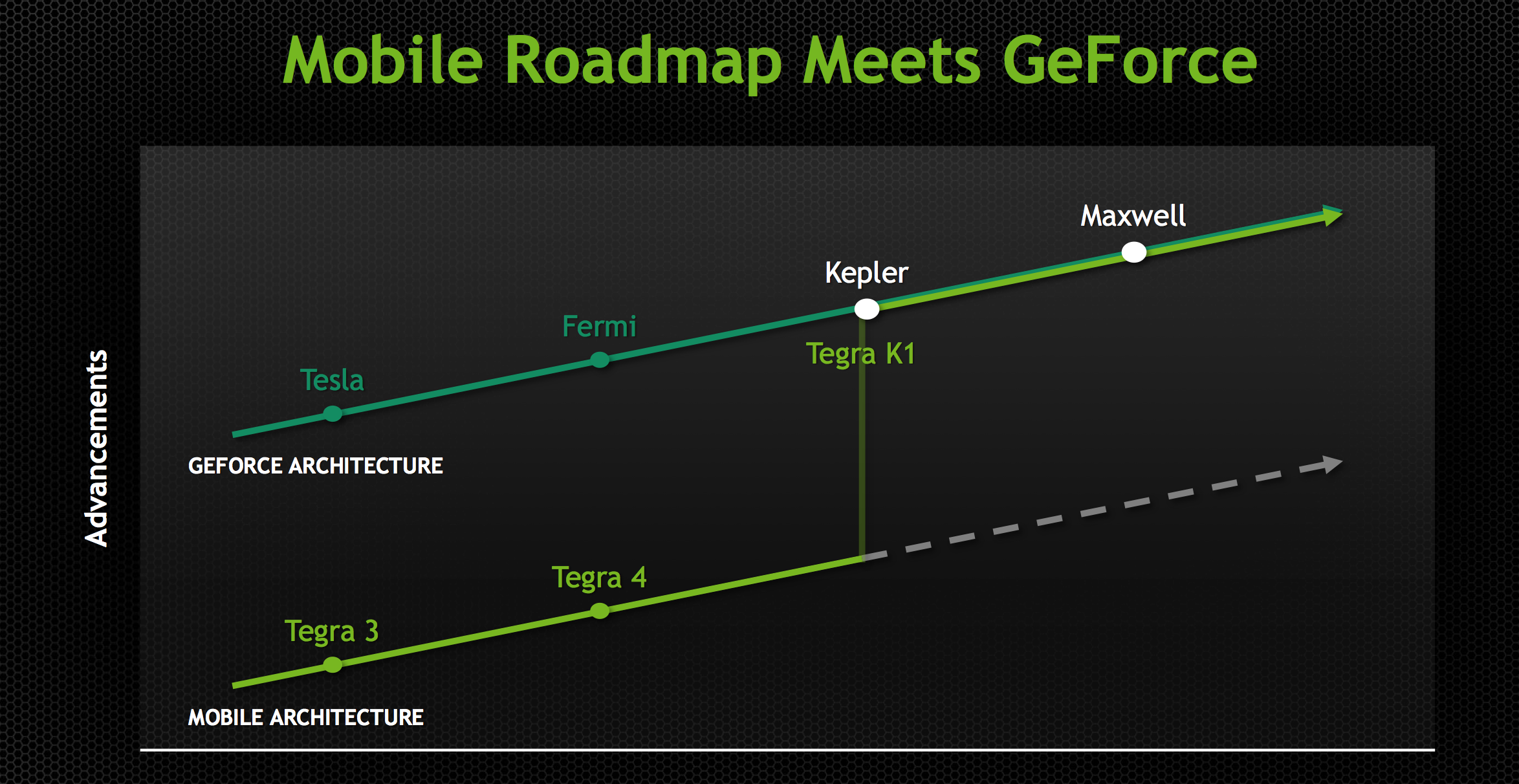
Kepler makes the move into mobile largely unchanged. This is a full Kepler implementation with the same size register file, shared L1 and is 100% ISA compatible with its big brother. It turns out that Kepler, as it was originally designed, was pretty good for mobile. If you take a GeForce 740M (2 SMX/384 CUDA core design), you’re looking at roughly a 19W GPU. Of that 19W, around 3W is memory IO, PCIe and other non-GPU things. You can subtract another 6W for leakage, bringing you down to 10W. Now that’s a 2 SMX design, so divide it in half and now you’re down to 5W. Drop the clock from 1GHz down to 900MHz, and the voltage as well, and now we’re talking around 2 - 3W for the GPU core and that’s without any re-architecting. Granted you can’t just subtract out things like leakage like that, but you get the point. Kepler wasn’t a bad starting point for a good mobile GPU design.
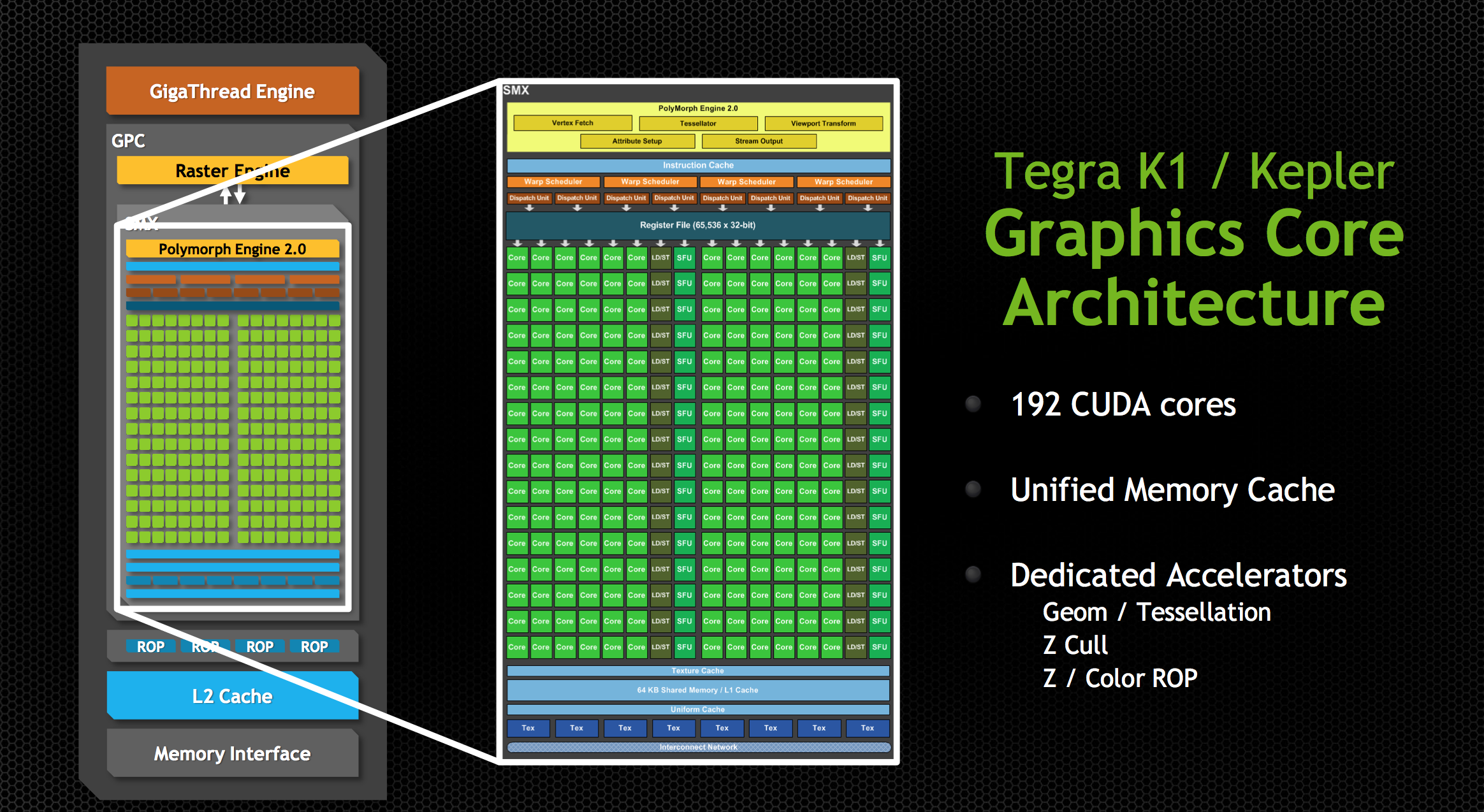
Tegra K1 features a single SMX (in a single GPC), which amounts to 192 CUDA cores. NVIDIA made the rookie mistake of calling Tegra K1 a 192-core processor, which made for some great headlines but largely does the industry a disservice.
Tessellation and geometry engines aren’t crippled compared to desktop Kepler. FP64 support is also present, at 1/24 the FP32 rate. There are 4 ROPs and 8 texture units, down from 16 in the PC version of Kepler. The big changes however are in the interconnects between all of the parts of the GPU.
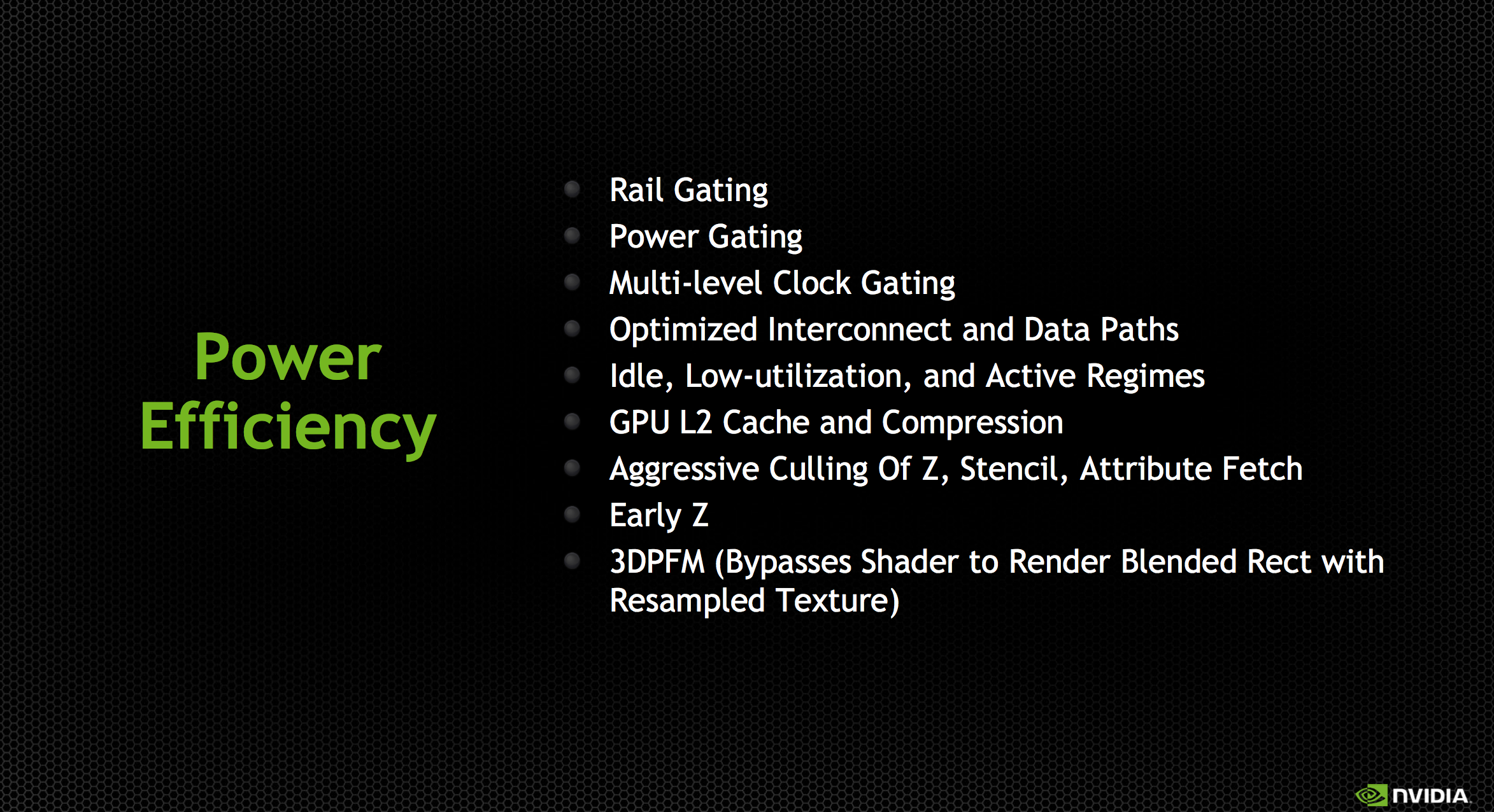
The bigger implementations of Kepler have to be able to efficiently move data between multiple SMXes, ROPs and memory controllers. The interconnect fabric needed to do that doesn’t scale down well for mobile, where in many cases we’re dealing with one or two of those things instead of a dozen. By removing the complexity that exists in the bigger Kepler’s fabric you limit the ability for mobile Kepler to scale, but then again mobile Kepler is never going to scale to the sizes of big desktop GPUs so it’s not an issue. There are other changes outside of interconnect, with improved clock gating among other focuses on power efficiency.
NVIDIA updated the texture units to support ASTC, something that isn’t present in the desktop Kepler variants at this point. NVIDIA also hopes to use the GPU’s color compression features to reduce memory bandwidth requirements in UI rendering and not just 3D games.

With the changes NVIDIA made to the design, Kepler ends up being a < 2W GPU perfect for mobile. NVIDIA provided us with some data showing SoC + DRAM power while running GFXBench 3.0 (Manhattan), an OpenGL ES 3.0 test:
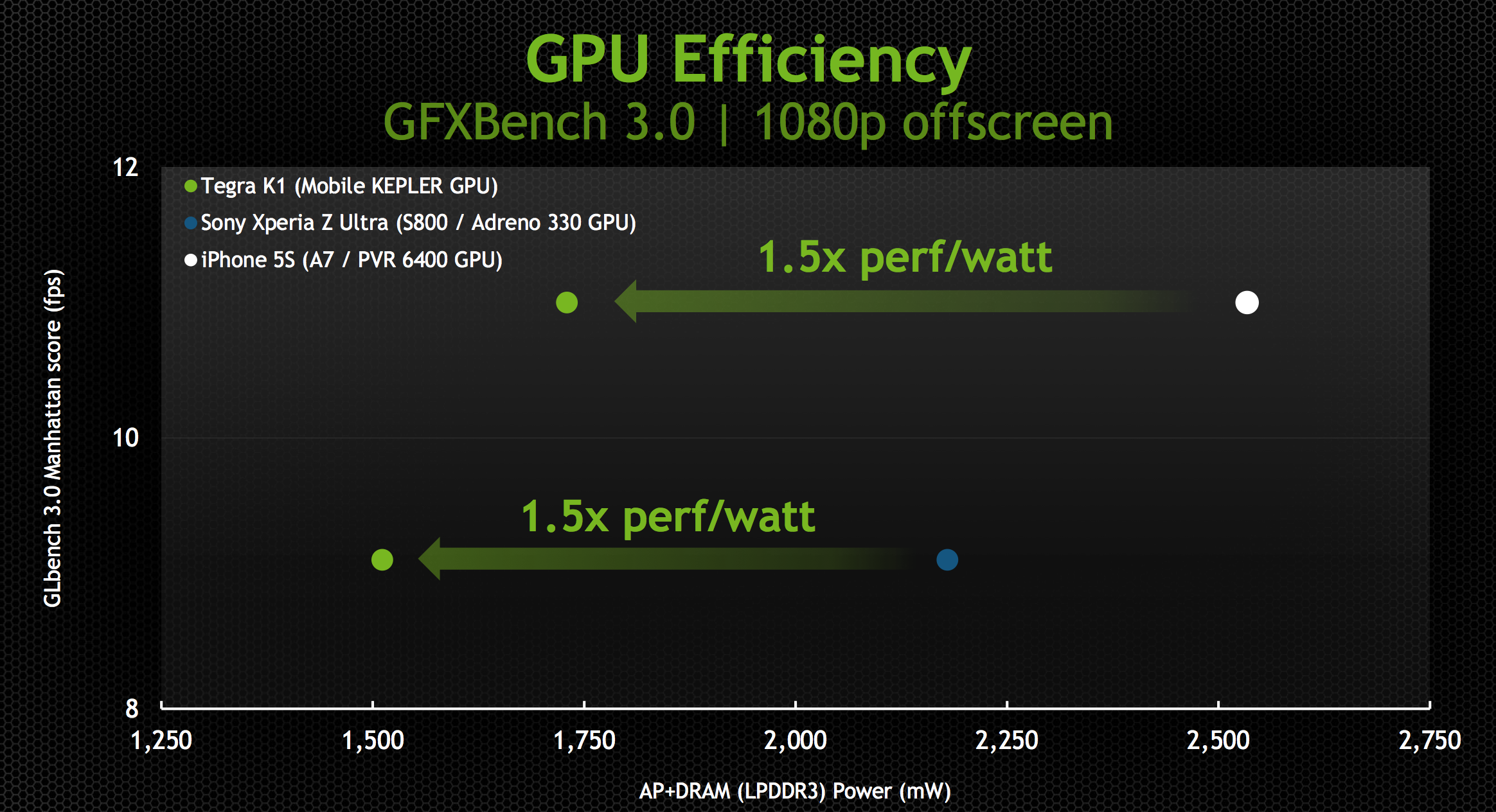
The data is presented in NVIDIA’s usual way where we’re not looking at peak performance but rather how Tegra K1 behaves when normalized to the performance of Apple’s A7 or Qualcomm’s Snapdragon 800. In both cases NVIDIA is claiming the ability to deliver equal performance at substantially better power efficiency.
NVIDIA shared some live demos that echoed the data above. Peak performance was capped to that of the A7 or Snapdragon 800, but SoC level power was always lower. It remains to be seen what power consumption looks like in a shipping configuration (which is almost always optimized for peak performance not equal performance at lower power), but it’s safe to say that concerns about Kepler being too power hungry for mobile are overrated.
The most compelling argument in favor of putting Kepler in a mobile SoC actually has to do with its API support. In one swift move NVIDIA goes from being disappointing in API support to industry leading. Since this is a full Kepler implementation (just a lower power/performing version) Tegra K1 maintains full API compatibility with NVIDIA’s flagship GeForce products. OpenGL ES 3.0 is supported but so are full OpenGL 4.4, DX11 and CUDA 6.0.

NVIDIA made it a point to say that high-end games developed for the PC or even current generation consoles could be ported over to Tegra K1 without issue. It’s perhaps over reaching a bit to claim the latter given the delta in performance (which NVIDIA hopes to make up in 4 generations!), but you can definitely argue that titles built for the previous generation of consoles (Xbox 360/PS3) could easily be ported to Tegra K1.
At its CES press conference NVIDIA teased the idea that Tegra K1 is actually more powerful than the last generation of consoles. The slide below attempts to drive that point home:
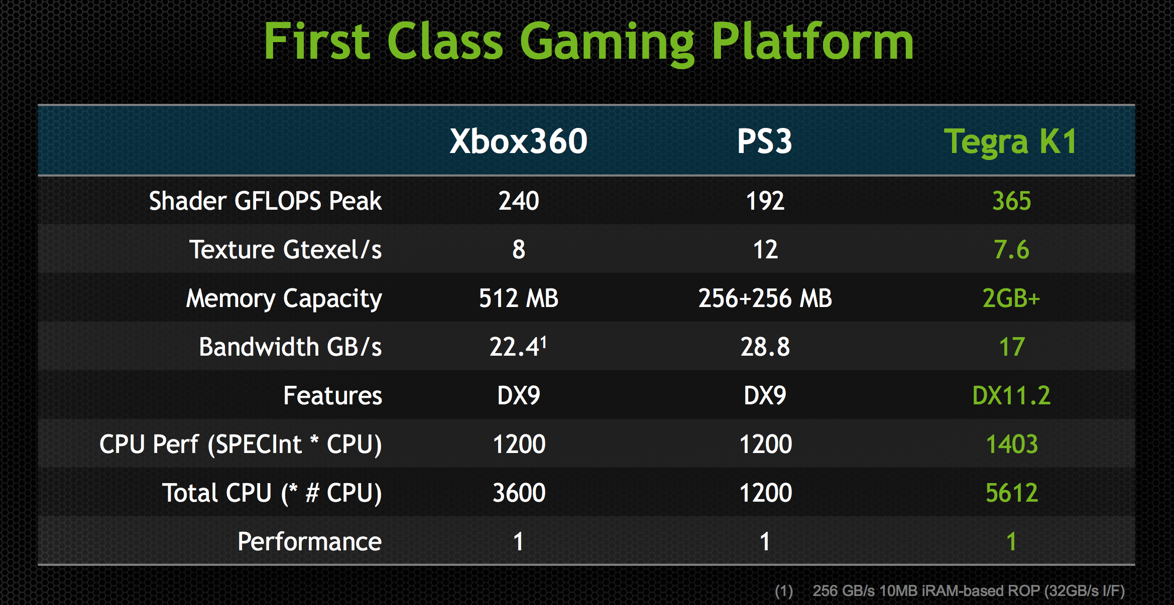
With a GPU clock of 950MHz (admittedly, a bit on the high end), NVIDIA can deliver substantially more raw horsepower than either previous generation console (192 CUDA cores * 2 FLOPS per core * 950MHz). Peak texture filtering performance and more importantly, memory bandwidth are lower than what was possible on these consoles but the numbers we’re talking about here aren’t substantial enough to prevent porting from happening. There may be some optimization needed but it definitely looks like Tegra K1 is the first mobile platform that can more or less run Xbox 360/PS3 titles, at least from a performance standpoint.
In pursuit of making porting and game development as simple as possible, NVIDIA demonstrated its NSight Tegra plugins for Visual Studio. Without changing the IDE that developers are used to, NSight Tegra allows developers to use the NDK toolchain all within Visual Studio. I’m not enough of a developer to know whether or not NVIDIA’s efforts in this space truly make life easy enough to port Xbox 360/PS3 games over to Android, but its VS integration demos looked convincing at least.
NVIDIA had a port of Serious Sam 3 running on Tegra K1 demo hardware just fine. Any games that are prepped for Steam OS are very easy to port over to Android. Once you make the move to OpenGL, the rest is allegedly fairly simple. The Serious Sam 3 port apparently took a matter of a couple of weeks to get ported over, with the bulk of the effort going into mapping controls to an Android environment.


88 Comments
View All Comments
blanarahul - Monday, January 6, 2014 - link
Quick question: Is it possible to build a 32-bit ARMv8 CPU core i.e. a ARMv8 core capable of running a 32-bit OS without using a hypervisor? That would really ease the transition to 64-bit for Android.blanarahul - Monday, January 6, 2014 - link
Anand, where do you find information about the revisions of Cortex cores??blanarahul - Monday, January 6, 2014 - link
Found it: http://infocenter.arm.com/help/index.jsp?topic=/co...klmx - Monday, January 6, 2014 - link
The real-time version of ARMv8 (ARMv8-R) is still 32-bit, and is capable of running a rich OS like Android, but I guess that's not the solution you had in minddroopaloop - Monday, January 6, 2014 - link
ARMv8 supports 2 different instruction sets; AArch32, and AArch64. AArch32 is basically the ARMv7 instruction set (read: 32bit). It is possible to run Android in AArch32. It is also possible to run the kernel in AArch64, and have AArch32 apps running on top which should help ease the transition to 64bit.Krysto - Monday, January 6, 2014 - link
How would using a 32-bit-only CPU ease the transition to 64-bit? ARMv8 supports both 32-bit and 64-bit modes by default (you can make it 64-bit-only later, though), so that's what needed for the "transition to be easier" - OEMs to just jump to ARMv8, even if the OS remains 32-bit.phoenix_rizzen - Monday, January 6, 2014 - link
This is exactly what Apple did with their A7 SoC. It's an ARMv8 CPU. It can run either a 64-bit or 32-bit version of iOS. If running the 64-bit version, it can run either 32-bit or 64-bit apps.Krysto - Monday, January 6, 2014 - link
That's what everyone will do. That's what I'm saying. It's the default. OEMs just need to switch to ARMv8, and that's it. It's up to Google to make Android 64-bit, and then to app devs to make their apps 64-bit, but neither is "necessary" for the transition to 64-bit CPUs.BMNify - Tuesday, January 7, 2014 - link
remember The Cortex-A15 and above also introduced full hardware accelerated virtualization so you could also run several versions of an OS concurrently too if you so wished and skillful enough to code your apps base libraries with good generic and fast inter process communications (xcore style)deltatux - Thursday, January 9, 2014 - link
Why would you need to build a 32-bit ARMv8 core? Android is highly portable, just recompile the entire thing to the aarch64 instruction set and you're good to go. Nearly all apps are written in Dalvik anyways which means you won't have to recompile those apps and ARMv8 in itself is backwards compatible with 32-bit just like how x86-64 is backwards compatible with the original 32-bit x86. So even if there are 32-bit native apps, they can easily run on 64-bit Android.NVIDIA has shown off Android 4.4 running on Denver in 64-bit mode, so 64-bit Android does exist and works out of the gate.