ATI’s Radeon 9700 (R300) – Crowning the New King
by Anand Lal Shimpi on July 18, 2002 5:00 AM EST- Posted in
- GPUs
By the time you read this, ATI still will not have decided on the clock speeds for the R300, but the card we tested was running at a core clock of 325MHz. Officially, ATI is shooting for above a 300MHz core clock and from our discussions with them it seems like they are realistically aiming for at least the 325MHz with which we tested.
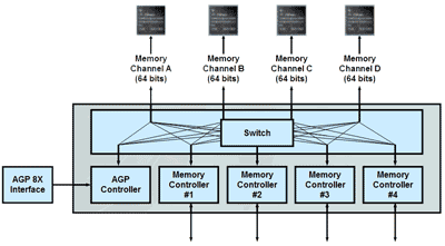
Like the Matrox Parhelia, the R300 supports a 256-bit DDR memory bus made up of four individual load-balanced 64-bit memory controllers à la NVIDIA’s Crossbar architecture. ATI is targeting memory clock speeds greater than 300MHz, and the board we tested ran at 310MHz DDR (effectively 620MHz). ATI is quick to point out that the R300 can support DDR-II, but we would expect that a slight redesign of the memory controller might be necessary to truly enable support. But we’ll talk about the future of the R300 much later in this article…
The rest of the R300 specs are as follows:
• 0.15-micron GPU
• 110+ million transistors
• 8 pixel rendering pipelines, 1 texture unit per pipeline, can do 16 textures per pass
• 4 programmable vect4 vertex shader pipelines
• 256-bit DDR memory bus
• up to 256MB of memory on board, clocked at over 300MHz (resulting in a minimum of 19.2GB/s of memory bandwidth)
• AGP 8X Support
• Full DX9 Pixel and Vertex Shader Support
• Single Full Speed 165MHz integrated TMDS transmitter
As we’ve started doing with our GPU overviews, we’ll take you through the R300 pipeline to help better explain the technology.


0 Comments
View All Comments