VIA Introduces Quad Band Memory - 2X DDR at 1X Prices
by Anand Lal Shimpi on September 17, 2002 1:49 PM EST- Posted in
- CPUs
The QBM Chipset Architecture
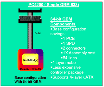
A chipset that supports Quad Band Memory (QBM) simply implements a conventional 64-bit DDR SDRAM memory interface with support in the memory controller for QBM modules. The obvious benefit of this is that the layout is no more complicated than any other motherboard with a single channel DDR interface, music to the ears of motherboard manufacturers. The bus interfaces to the same 184-pin DDR SDRAM slots we've been seeing on boards for years now.
Instead of putting the burden on motherboard manufactures to implement a dual channel DDR memory bus, the burden is placed on the memory manufacturers to produce special QBM modules. We'll get to exactly how these modules are made in a minute, but first let's talk about one of the benefits of the QBM chipset design.
Because of the pin-compatible DDR interface, QBM chipsets will be able to use both regular DDR SDRAM modules as well as QBM modules. Obviously regular DDR modules will offer lesser amounts of memory bandwidth but the backwards compatibility means that motherboard manufacturers would be able to produce one board for multiple segments (single channel DDR for mainstream and QBM for high end).
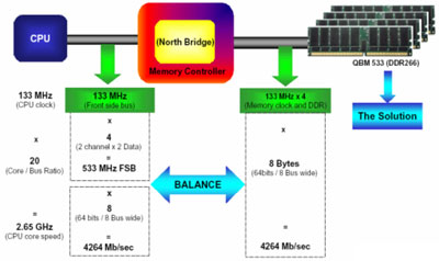
But what exactly do QBM modules do and how do they offer more memory bandwidth over the same 64-bit bus as DDR SDRAM? The explanation is actually quite simple…


0 Comments
View All Comments