FIC AZ11E Socket-A KT133 (686B) ATX
by Henry Kuo on November 15, 2000 12:00 PM EST- Posted in
- Motherboards
The VIA KT133 chipset has supported the AMD Thunderbird and Duron series of processors since their launch a little more than 4 months ago. It has been doing a fine job of delivering the power of those processors. At the same time, AMD has been working on their 760 chipset. Four months later, AMD finally revealed the chipset, which features support for DDR SDRAM and "266MHz" FSB processors. Nonetheless, the chipset still supports the good old 200MHz Thunderbird and Duron processors.
The new AMD 760 chipset definitely helps to bring out more from the processors than the VIA KT133 chipset, for more information read our AMD 760 Chipset Review. However, there are still quite a few questions to be answered. When will motherboards with 760 chipset be out? How much would they cost? Will the DDR memory market be able to keep up with the demand? And above all, you will have to live with the fact that their PC100 or PC133 memory will be useless on the new boards.
All the above reasons prove that it is not time for KT133 to retire yet, and that's exactly when we are seeing with the second wave of KT133 motherboards coming out. They come with multiplier ratio settings, Ultra ATA 100 support, or even on-board IDE RAID controller.
FIC was among the first to release their KT133 solution, the AZ11, but it was not a particularly outstanding board. This time around they have the AZ11E, which is an enhanced version of the AZ11, with more features and better performance. Being a big supporter for AMD, how would FIC compare among the second wave of KT133 motherboards? Let's see how the AZ11E stands up under the AnandTech microscope.
|
FIC AZ11E Specifications |
|
| CPU Interface |
Socket-A
|
| Chipset |
VIA
KT133
VIA 8363 North Bridge VIA 686B Super South Bridge |
| L2 Cache |
N/A
(on-chip)
|
| Form Factor |
ATX
|
| Bus Speeds |
90
/ 95 / 100 / 101 / 102 / 103 / 105 / 107 / 109 / 110
111 / 113 / 115 / 117 / 120 / 125 / 130 / 133 135 / 137 / 139 / 140 / 143 / 145 / 148 / 150 / 155 / 166 |
| Voltages Supported |
Auto
Detect
1.475 - 1.850 V (in 0.025V increments) |
| Memory Slots |
3
168-pin DIMM Slots
|
| Expansion Slots |
1 AGP Slot
5 PCI Slots (3 Full Length) 1 CNR Slot (0 Shared) 0 ISA Slots |
| Onboard Sound |
Sigmatel
STAC9700T AC 97 CODEC
|
| BIOS |
Award
Modular BIOS 6.00PG
|
The Good
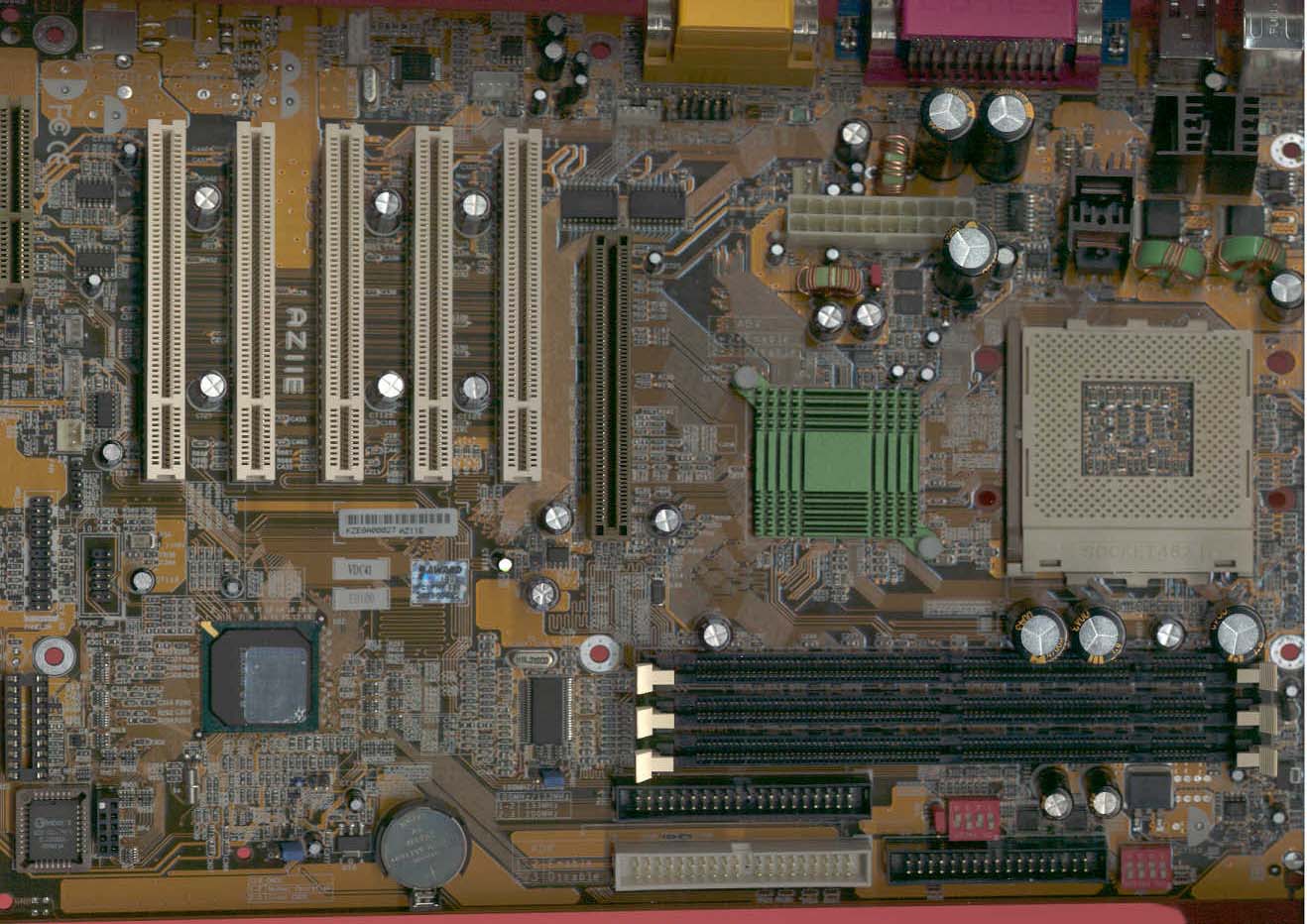
When you first look at the AZ11E, it is immediately obvious that it is very different from the AZ11. With the AZ11, most of the left side of the PCB was left blank, but that is not the case with AZ11E. And you can see that the layout of the board is very different, meaning that FIC has spent quite a bit of effort optimizing the routing of traces. The fact that the AZ11E was much more stable in our tests shows that FIC's efforts have paid off. Unfortunately, the AZ11E still utilizes a relatively large PCB, around 12 by 9 inches. FIC did not include any features that would require such a large PCB, so it's a bit of a surprise that they've stuck with such a design since a larger PCB has the disadvantage of not fitting in some smaller cases and also increases the overall cost to manufacture the board. Of course, that cost is passed on to the consumer in one way or another.
The ATX power supply connector is placed next to the serial / parallel ports and some large capacitors. As processors generate more and more heat, ventilation around the CPU has become especially important for good cooling. Having the power supply connector at where it is now means that the power cables will have to run over the memory and the CPU, thus potentially blocking airflow. So far the best place for the connector is the right edge of the PCB or next to the DIMM slots, where the power cables can avoid running over the CPU.
During the first wave of KT133 motherboards, ABIT and ASUS won out simply thanks to their ability to change the multiplier ratios of the processor for overclocking purposes. But that has all changed as more and more boards have arrived with that feature, including the Soyo K7VTA, MSI K7T Pro2 and now the AZ11E. In our AMD Thunderbird & Duron Overclocking Revealed article, we discussed the fact that the AZ11 actually had the ability to change the multiplier of the processors, but FIC decided to leave out the required hardware and jumpers.
 Sure
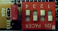
enough FIC is not going to let this slip by with their AZ11E. They implemented
a set of ADR (Auto Detect Frequency Ratio) dipswitches that allow you to select
multiplier ratios between 5 and 12.5 in 0.5 increments. Dipswitches are fine,
but we would prefer to have the settings done inside the BIOS, like on the ABIT
KT7-RAID or the Microstar K7T Pro2.
Sure
enough FIC is not going to let this slip by with their AZ11E. They implemented
a set of ADR (Auto Detect Frequency Ratio) dipswitches that allow you to select
multiplier ratios between 5 and 12.5 in 0.5 increments. Dipswitches are fine,
but we would prefer to have the settings done inside the BIOS, like on the ABIT
KT7-RAID or the Microstar K7T Pro2.
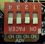 FIC
also provides a wide range of CPU core voltage setting for users between 1.475V
and 1.850V in 0.025V increments. However, just like the multiplier ratio settings,
FIC implemented them with a set of ADV (Auto Detect CPU core Voltage) dipswitches.
Usually, you will raise the core voltage step by step to be sure that you do
not damage the CPU - having these settings controlled by dipswitches will further
complicate an already complicated procedure for many. It would be much better
if FIC implemented the settings inside the BIOS - something that most other
manufacturers have done.
FIC
also provides a wide range of CPU core voltage setting for users between 1.475V
and 1.850V in 0.025V increments. However, just like the multiplier ratio settings,
FIC implemented them with a set of ADV (Auto Detect CPU core Voltage) dipswitches.
Usually, you will raise the core voltage step by step to be sure that you do
not damage the CPU - having these settings controlled by dipswitches will further
complicate an already complicated procedure for many. It would be much better
if FIC implemented the settings inside the BIOS - something that most other
manufacturers have done.
Fortunately, the FIC AZ11E takes advantage of the jumperless functions in the Award Modular BIOS 6.00PG for the FSB settings. The FSB settings available to users are 90 / 95 / 100 / 101 / 102 / 103 / 105 / 107 / 109 / 110 / 111 / 113 / 115 / 117 / 120 / 125 / 130 / 133 / 135 / 137 / 139 / 140 / 143 / 145 / 148 / 150 / 155 / 166 MHz. Ideally it would be nice if FIC had provided settings in 1MHz increments between 100MHz and 110MHz, if not all the way up to 166MHz, but the available settings should be enough for most users to overclock their AMD processors. As we've noted in the past, the KT133 chipset is not stable above 110MHz FSB in the vast majority of cases, although mileage will vary.
We used an AMD Thunderbird 800MHz OEM CPU for our overclocking test. By staying with the default voltage and 100MHz FSB, we again achieved a multiplier setting of 9.5 before the system lost stability. Then we were able to raise the FSB to 105MHz, which finally yield a clock speed on 997.5MHz (105MHz x 9.5). After several boards with multiplier ratio settings, it seems that reaching 997.5MHz is the limit of our particular chip and cooling. It probably means that the motherboards are able to push the chips further provided we had better cooling. Also notice that we did not change our default voltage, in the interest of keeping things fair, which would have also helped our overclocking efforts.


0 Comments
View All Comments