TSMC
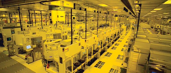
With all the new fabs being built in Germany and Japan, as well as the expansion of production capacity in China, TSMC is planning to extend its production capacity for specialty technologies by 50% by 2027. As disclosed by the company during its European Technology Symposium this week, TSMC expects to need to not only convert existing capacity to meet demands for specialty processes, but even build new (greenfield) fab space just for this purpose. One of the big drivers for this demand, in turn, will be TSMC's next specialty node: N4e, a 4nm-class ultra-low-power production node. "In the past, we always did the review phase [for upcoming fabs], but for the first time in a long time at TSMC, we started building greenfield fab...

TSMC’s 5nm EUV Making Progress: PDK, DRM, EDA Tools, 3rd Party IP Ready
TSMC this week has said that it has completed development of tools required for design of SoCs that are made using its 5 nm (CLN5FF, N5) fabrication technology. The...
33 by Anton Shilov on 4/5/2019
TSMC’s Fab 14B Photoresist Material Incident: $550 Million in Lost Revenue
TSMC on Friday revealed more details regarding an incident with a photoresist material at its Fab 14B earlier this year. The contaminated chemical damaged wafers on TSMC’s 12 nm...
29 by Anton Shilov on 2/20/2019
TSMC Chip Yields Hit By Bad Chemical Batch
TSMC on Monday said that some of the wafers it has processed recently have lower yields because of a chemical it uses during production. The company began investigation and...
28 by Anton Shilov on 1/29/2019
ASML to Ship 30 EUV Scanners in 2019: Faster EUV Tools Coming
ASML said last week that it planned to ship 30 extreme ultraviolet scanners in 2019, up significantly from 2018. The plan is not surprising, as demand for EUV lithography...
17 by Anton Shilov on 1/28/2019
TSMC: 7nm Now Biggest Share of Revenue
As process node technology gets ever more complex, it costs big dollars to develop and then building chips on the process is also a very costly process. The big...
44 by Ian Cutress on 1/17/2019
TSMC: First 7nm EUV Chips Taped Out, 5nm Risk Production in Q2 2019
Last week, TSMC made two important announcements concerning its progress with extreme ultraviolet lithography (EUVL). First up, the company has successfully taped out its first customer chip using its...
50 by Anton Shilov on 10/9/2018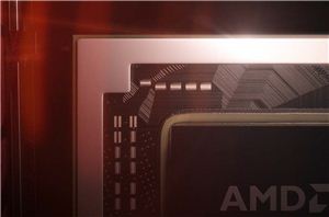
AMD's 7nm CPUs & GPUs To Be Fabbed by TSMC, on Track for 2018 - 2019
With the announcement that its long-time manufacturing partner (and outright former fab) GlobalFoundries is dropping out of the race for bleeding-edge manufacturing nodes, the second big question of the...
28 by Ryan Smith & Anton Shilov on 8/27/2018
TSMC: Outbreak of Malware That Triggered Delays & Losses Caused by Software for New Tool
TSMC announced this week that it suffered a computer malware outbreak, resulting in a roughly 3 day outage for parts of the fab while systems were restored. As a...
42 by Anton Shilov on 8/9/2018
AMD “Rome” EPYC CPUs to Be Fabbed By TSMC
Along with AMD’s epic quarterly results that were announced yesterday afternoon, there was also an interesting nugget buried in the earnings call for the results. We’ve known for some...
32 by Ryan Smith on 7/26/2018
TSMC Details 5 nm Process Tech: Aggressive Scaling, But Thin Power and Performance Gains
At a special event last week, TSMC announced the first details about its 5 nm manufacturing technology that it plans to use sometime in 2020. CLN5 will be the...
10 by Anton Shilov on 5/8/2018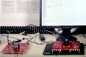
Cadence and Micron Demo DDR5-4400 IMC and Memory, Due in 2019
Cadence this week introduced the industry’s first IP interface in silicon for the current provisional DDR5 specification developed by JEDEC. Cadence’s IP and test chip us fabricated using TSMC’s...
31 by Anton Shilov on 5/3/2018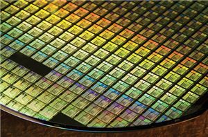
TSMC Kicks Off Volume Production of 7nm Chips
TSMC last week announced that it had started high volume production (HVM) of chips using their first-gen 7 nm (CLN7FF) process technology. The contract maker of semiconductors says it...
63 by Anton Shilov on 4/24/2018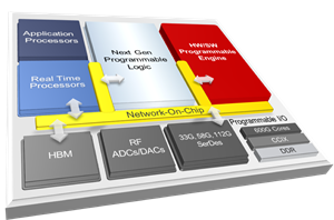
Xilinx Announces Project Everest: The 7nm FPGA SoC Hybrid
This week Xilinx is making public its latest internal project for the next era of specialized computing. The new product line, called Project Everest in the interim, is based...
16 by Ian Cutress on 3/19/2018
TSMC Starts to Build Fab 18: 5 nm, Volume Production in Early 2020
TSMC last week held a groundbreaking ceremony for its Fab 18 phase 1 production facility. The fab will produce chips using TSMC’s 5 nm process starting from early 2020...
27 by Anton Shilov on 1/31/2018
Getting Radeon Vega Everywhere: An Exclusive Media Interview at AMD Tech Day, with CEO Dr. Lisa Su
In what is becoming an annual tradition, during AMD’s Tech Day here at CES we were given the opportunity to spend some time with Dr. Lisa Su, AMD’s CEO...
65 by Ian Cutress on 1/24/2018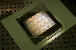
TSMC Teams Up with ARM and Cadence to Build 7nm Data Center Test Chips in Q1 2018
TSMC has announced plans to build its first test chips for data center applications using its 7 nm fabrication technology. The chip will use compute cores from ARM, a...
12 by Anton Shilov on 9/14/2017
Microsoft’s Project Scorpio: More Hardware Details Revealed
This news piece contains speculation, and suggests silicon implementation based on released products and roadmaps. The only elements confirmed for Project Scorpio are the eight x86 cores, 6 TFLOPs...
113 by Ian Cutress on 4/6/2017
ARM Announces 10FF "Artemis" Test Chip
Today in collaboration with TSMC, ARM's physical IP division is announcing the tapeout of a 10nm test chip demonstrating the company's readiness for the new manufacturing process. The new...
24 by Andrei Frumusanu on 5/18/2016
EUV Lithography Makes Good Progress, Still Not Ready for Prime Time
At the recent annual SPIE Advanced Lithography conference, Intel, TSMC and other leading semiconductor companies said that significant strides have been made in extreme ultraviolet lithography (EUVL) over the...
38 by Anton Shilov on 3/10/2016


