NVIDIA's GeForce 8800 (G80): GPUs Re-architected for DirectX 10
by Anand Lal Shimpi & Derek Wilson on November 8, 2006 6:01 PM EST- Posted in
- GPUs
G80: A Mile High Overview
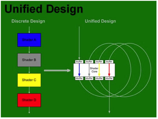
Now that we know a little more about the requirements and direction of DX10, we can take a deeper look at where NVIDIA has decided to go with the architecture of G80. We will be seeing a completely new design based around a unified shader architecture. While DX10 doesn't require a unified architecture, it certainly does make a lot of sense to move in that direction.
Inside G80, vertex, geometry, pixel shaders and more (more on this later) are all able to run on the same set of execution resources. In order to make this happen, the shader core needed to be made more general purpose and suitable for multiple usage scenarios. This is much like what we are used to seeing on a CPU, and as time moves on we expect these similarities to increase from both the CPU and GPU side. The design NVIDIA has come up, while very complex and powerful, is quite elegant. Here's a look at the block diagram for G80:
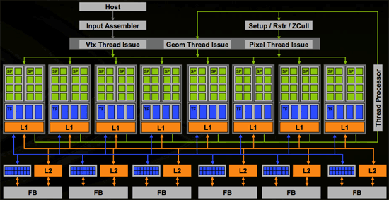
The architecture is able to use thread management hardware to dispatch different types of instructions on to the shader core. As vertices complete, their output can be used as input to geometry shaders back at the "top" of the shader core. Geometry shader output is then used as input to pixel shaders. Here's a quick conceptual representation of what we are talking about:
The sheer size of G80 is absolutely amazing; while NVIDIA wouldn't disclose exact die sizes let's look at the facts. The G80 chip is made up of 681 million transistors, more than a single core Itanium 2 or the recently launched Kentsfield, but manufactured on an almost old 90nm process. As a reference point, ATI's Radeon X1900 XTX based on the R580 GPU was built on a 90nm process yet it featured only 384 million transistors. NVIDIA's previous high-end GPU, the G71 based GeForce 7900 GTX was also built on a 90nm process but used only 278 million transistors. Any way you slice it, this is one huge chip. Architecting such a massive GPU has taken NVIDIA a great deal of time and money, four years and $475M to be exact. The previous record for time was almost 3 years at a lesser amount, but NVIDIA wouldn't tell us which GPU that was.
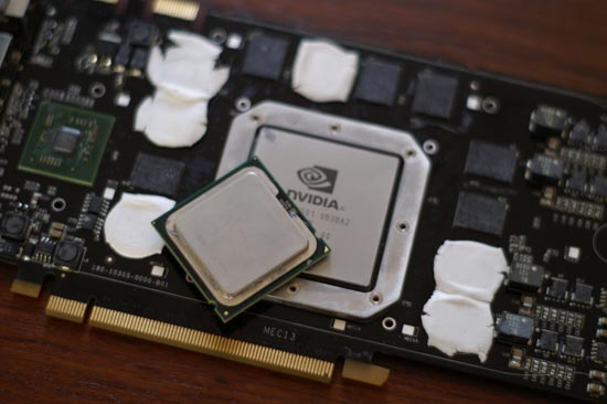
Intel's Quad Core Kentsfield on top, G80 on bottom
Despite very high clock speeds on the die and a ridiculous 681 million transistor count, power consumption of NVIDIA's G80 is quite reasonable given its target; on average, a G80 system uses about 8% more power than one outfitted with ATI's Radeon X1950 XTX.
You really start to get a sense of how much of a departure G80 is from previous architectures when you look at the shader core. Composed of 128 simple processors, called Stream Processors (SPs), the G80 shader core runs at a very high 1.35GHz on the highest end G80 SKU. We'll get into exactly what these stream processors are on the coming pages, but NVIDIA basically put together a wide array of very fast, specialized, but simple processors. In a sense, G80's shader core looks much like Cell's array of SPEs, but the SPs here are not nearly as independent as the SPEs in Cell.
Running at up to 1.35GHz, NVIDIA had to borrow a few pages from the books of Intel in order to get this done. The SPs are fairly deeply pipelined and as you'll soon see, are only able to operate on scalar values, thus through simplifying the processors and lengthening their pipelines NVIDIA was able to hit the G80's aggressive clock targets. There was one other CPU-like trick employed to make sure that G80 could have such a shader core, and that is the use of custom logic and layout.
The reason new CPU architectures take years to design while new GPU architectures can be cranked out in a matter of 12 months is because of how they're designed. GPUs are generally designed using a hardware description language (HDL), which is sort of a high level programming language that is used to translate code into a transistor layout that you can use to build your chip. At the other end of the spectrum are CPU designs which are largely done by hand, where design is handled at the transistor level rather than at a higher level like a HDL would.
Elements of GPUs have been designed at the transistor level in the past; things like memory interfaces, analog circuits, memories, register files and TMDS drivers were done by hand using custom transistor level design. But shaders and the rest of the pipeline was designed by writing high level HDL code and relying on automated layout.
You can probably guess where we're headed with this; the major difference between G80 and NVIDIA's previous GPUs is that NVIDIA designed the shader core at the transistor level. If you've heard the rumors of NVIDIA building more than just GPUs in the future, this is the first step, although NVIDIA was quick to point out that G80 won't be the norm. NVIDIA will continue to design using HDLs where it makes sense, and in critical areas where additional performance or power sensitive circuitry is needed, we'll see transistor level layout work done by NVIDIA's engineering. It's simply not feasible for NVIDIA's current engineering staff and product cycles to work with a GPU designed completely at the transistor level. That's not to say it won't happen in the future, and if NVIDIA does eventually get into the system on a chip business with its own general purpose CPU core, it will have to happen; but it's not happening anytime soon.
The additional custom logic and layout present in G80 helped extend the design cycle to a full four years and brought costs for the chip up to $475M. Prior to G80 the previous longest design cycle was approximately 2.5 - 3 years. Although G80 did take four years to design, much of that was due to the fact that G80 was a radical re-architecting of the graphics pipeline and that future GPUs derived from G80 will have an obviously shorter design cycle.


111 Comments
View All Comments
Nightmare225 - Sunday, November 26, 2006 - link
Are the FPS posted in this article, Minimum FPS, Average FPS, or Maximum? Thanks!multiblitz - Monday, November 20, 2006 - link
I enjoyed your reviews always a lot as they inclueded the video-capbilities for a HTPC on previous cards. Unfortunately this was this time not the case. Hopefully there will be a 2. Part covering this as well ? If so, it would be nice to make a compariosn on picture quality as well against the filters of ffdshow, as nvidia is now as well supporting postprocessing filters...DerekWilson - Tuesday, November 21, 2006 - link
What we know right now is that 8800 gets a 128 out of 130 on HQV tests.We haven't quite put together an HTPC look at 8800, but this is a possibility for the future.
epsil0n - Sunday, November 19, 2006 - link
I am not agree with this:"It isn't surprising to see that NVIDIA's implementation of a unified shader is based on taking a pixel shader quad pipeline, and breaking up the vector units into 4 scalar units. Now, rather than 4 pixel quads, we see 16 SPs per "quad" or block of stream processors. Each block of 16 SPs shares 4 texture address units, 8 texture filter units, and an L1 cache."
If i understood well this sentence tells that given 4 pixels the numbers of SPs involved in the computation are 16. Then, this assumes that each component of the pixel shader is computed horizontally over 16 SP (4pixel x 4rgba = 16SP). But, are you sure??
I didn't found others articles over the web that speculate about this. Reading others articles the main idea that i realized is that a shader is computed by one and only one SP. Each vector instruction (inside the shader) is "mapped" as a sequence of scalar operations (a dot product beetwen two vectors is mapped as 4 MUD/ADD operations). As a consequence, in this scenario 4 pixels are computed only by 4 SPs.
DerekWilson - Tuesday, November 21, 2006 - link
Honestly, NVIDIA wouldn't give us this level of detail. We certainly pressed them about how vertices and pixels map to SPs, but the answer we got was always something about how dynamic the hardware is able to dynamically schedule the SPs optimally according to what needs to be done.They can get away with being obscure about how they actually process the data because it could happen either way and provide the same effect to the developer and gamer alike.
Scheduling the simultaneous processing one vec4 MAD operation on 4 quads (16 pixels) over 4 groups of 4 SPs will take 4 clock cycles (in terms of throughput). Processing the same 16 pixels on 16 SPs will also take 4 clock cycles.
But there are reasons to believe that things happen the way we described. Loading components of 16 different "threads" (verts, pixels or whatever) would likely be harder on the cache than loading all 4 components of 4 different threads. We could see them schedule multiple ops from 4 threads to fill up each block of shaders -- like computing 4 consecutive scalar operations for 4 threads on 16 SPs.
At the same time, it might be easier to maximize SP utilization if 16 threads were processed on one block of SPs every clock.
I think the answer to this question is that NVIDIA knows, they didn't tell us, and all we can do is give it our best guess.
xtknight - Thursday, November 16, 2006 - link
This has been AT's best article in awhile. Tons of great, concise info.I have a question about the gamma corrected AA. This would be detrimental if you've already calibrated your display, correct (assuming the game heeds to the calibration)? Do you know what gamma correction factor the cards use for 'gamma corrected AA'?
DerekWilson - Monday, November 20, 2006 - link
I don't know if they dynamically adjust gamma correction based on monitor (that would be nice though) ...if they don't they likely adjusted for a gamma of either (or between) 2.2 or 2.5.
Also, thanks :-) There was a lot more we wanted to pack in, but I'm glad to see that we did a good job with what we were able to include.
Thanks,
Derek Wilson
bjacobson - Sunday, November 12, 2006 - link
This comment is unrelated, but could you implement some system where after rating a comment, on reload the page goes back to the comment I was just at? Otherwise I rate something halfway down and then have to spend several seconds finding where I just was. Just a little nuissance.Thanks for the great article, fun read.
neo229 - Friday, November 10, 2006 - link
This is a very suspect quote. A card that requires two PCIe power connectors is going to dissipate a lot of heat. More heat means there must be a faster, louder fan or more substantial and costly heat sink. The extra costs associated with providing a truly quiet card mean that the bulk of manufacturers go with the loud fan option.
DerekWilson - Friday, November 10, 2006 - link
If manufacturers go with the NVIDIA reference design, then we will see a nice large heatsink with a huge quiet fan.Really, it does move a lot of air without making a lot of noise ... Are there any devices we can get to measure the airflow of a cooling solution?
We are also seeing some designs using water cooling and theres even one with a thermo-electric (peltier) cooler on it. Manufacturers are going to great lengths to keep this thing running cool without generating much noise.
None of the 8 retail cards we are testing right now generate nearly the noise of the X1950 XTX ... We are working on a retail roundup right now, and we'll absolutely have noise numbers for all of these cards at load.