Overclocking
As we mentioned before, the ASUS V7100 that we received was overclocked upon shipping. The core was running at 180 MHz and the memory at 171 MHz, proving for a very conservative overclock. There is almost no question that every V7100 out there should be able to run at these speeds, regardless of whether or not it ships like that.
The heatsink attached to the GPU is quite a plus for overclocking the V7100's core. Even without any cooling, we were able to get our previously reviewed VisionTek GeForce2 MX card up to 200 MHz so it was no surprise that our V7100 overclocked even higher. We were able to reach a core speed of 210 MHz on our V7100. This seems like the logical place of a passively cooled GeForce2 MX core to be, as our Overclocking the GeForce2 MX guide showed that with active cooling the MX was able to get up to 220 MHz. The passively cooled V7100 lies right in the middle of these two solutions, with a core speed of 210 MHz.
 The
problem is that overclocking the core, as easy as it may be, does not provide
any significant performance increase due to the memory bandwidth limitations
as a result of the SDR memory used. ASUS must have been pretty confident about
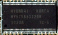
the Hyundai parts found on our V7100, as they were clocked 5 MHz above the memory's
rated speed. Once again, this overclock is very conservative and it is likely
that almost every 6ns Hyundai RAM chip sold will be able to clock at this speed.
Once we pushed the memory as high as it could go, we found that our board was
able to reach a memory speed of 210 MHz. As with all MX based cards, the faster
the memory the better, so even faster memory (such as 5.5ns) is preferable since
they will be able to overclock even higher than the 6ns samples found on our
board.


0 Comments
View All Comments