TSMC
Taiwan Semiconductor Manufacturing Co. this week said its revenue for the second quarter 2024 reached $20.82 billion, making it the company's best quarter (at least in dollars) to date. TSMC's high-performance computing (HPC) platform revenue share exceeded 52% for the first time in many years due to demand for AI processors and rebound of the PC market. TSMC earned $20.82 billion USD in revenue for the second quarter of 2024, a 32.8% year-over-year increase and a 10.3% increase from the previous quarter. Perhaps more remarkable, $20.82 billion is a higher result than the company posted Q3 2022 ($20.23 billion), the foundry's best quarter to date. Otherwise, in terms of profitability, TSMC booked $7.59 billion in net income for the quarter, for a gross margin of...
EUV Pellicles Ready For Fabs, Expected to Boost Chip Yields and Sizes
Foundries started limited usage of extreme ultraviolet (EUV) lithography for high-volume manufacturing (HVM) of chips in 2019. At the time, ASML's Twinscan NXE scanners were good enough for production...
35 by Anton Shilov on 3/31/2021
Intel’s x86 Designs No Longer Limited to Intel on Intel: IP Blocks for Foundry, Cores on TSMC
Today Intel’s CEO Pat Gelsinger has outlined two key changes to Intel policy: one derived from Intel’s plans to offer foundry services to external partners, and the other from...
70 by Dr. Ian Cutress on 3/23/2021
Report: Semi Demand 30% Above Supply, 20% Year-on-Year Growth
Semiconductor foundry offerings are thriving due to unprecedented demand for semiconductors and processors in recent quarters. Analysts from TrendForce believe that in Q1 2021 foundries will increase their revenue...
31 by Anton Shilov on 2/25/20212_waifu2x_photo_noise2_scale_tta_1_carousel.jpg)
Xbox Series X SoC: Power, Thermal, and Yield Tradeoffs
This week at ISSCC (International Solid State Circuits Conference), Microsoft presented a talk titled ‘Xbox Series X SoC: A Next Generation Gaming Console’, with hardware engineer Paul Paternoster presenting...
82 by Dr. Ian Cutress on 2/15/2021
AMD Reports Q4 2020 Earnings: Analyst Q&A Transcript
At the end of every financial call, invited financial analysts have an opportunity to probe the key members of the company on the numbers, as well as future products...
11 by Dr. Ian Cutress on 1/26/2021Marvell Announces 112G SerDes, Built on TSMC 5nm
So far we have three products in the market built on TSMC’s N5 process: the Huawei Kirin 9000 5G SoC, found in the Mate 40 Pro, the Apple A14...
15 by Dr. Ian Cutress on 11/17/2020
AMD Zen 3: An AnandTech Interview with CTO Mark Papermaster
The announcement of the new Ryzen 5000 processors, built on AMD’s Zen 3 microarchitecture, has caused waves of excitement and questions as to the performance. The launch of the...
202 by Dr. Ian Cutress on 10/16/2020
AMD Zen 3 Announcement by Lisa Su: A Live Blog at Noon ET (16:00 UTC)
One of the most anticipated launches of 2020 is now here. AMD's CEO, Dr. Lisa Su, is set to announce and reveal the new Ryzen 5000 series processors using...
90 by Dr. Ian Cutress on 10/8/2020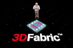
3DFabric: The Home for TSMC’s 2.5D and 3D Stacking Roadmap
Interposers. EMIB. Foveros. Die-to-die stacking. ODI. AIB.TSVs. All these words and acronyms have one overriding feature – they are all involved in how two bits of silicon physically connect...
9 by Dr. Ian Cutress on 9/2/2020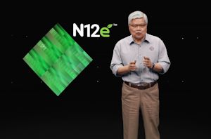
TSMC Launches New N12e Process: FinFET at 0.4V for IoT
One of the main drivers for the semiconductor industry is the growth in always-connected devices that require silicon inside, either for compute, communication, or control. The ‘Internet of Things&rsquo...
27 by Dr. Ian Cutress on 8/27/2020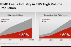
TSMC: We have 50% of All EUV Installations, 60% Wafer Capacity
One of the overriding central messages to TSMC’s Technology Symposium this week is that the company is a world leader in semiconductor manufacturing, especially at the leading edge process...
32 by Dr. Ian Cutress on 8/27/2020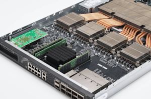
TSMC and Graphcore Prepare for AI Acceleration on 3nm
One of the side announcements made during TSMC’s Technology Symposium was that it already has customers on hand with product development progressing for its future 3nm process node technology...
2 by Dr. Ian Cutress on 8/27/2020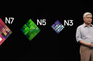
Where are my GAA-FETs? TSMC to Stay with FinFET for 3nm
As we passed that 22nm to 16nm barrier, almost all the major semiconductor fabrication companies on the leading edge transitioned from planar transistors to FinFET transistors. The benefits of...
37 by Dr. Ian Cutress on 8/26/2020
2023 Interposers: TSMC Hints at 3400mm2 + 12x HBM in one Package
High-performance computing chip designs have been pushing the ultra-high-end packaging technologies to their limits in the recent years. A solution to the need for extreme bandwidth requirements in the...
35 by Andrei Frumusanu on 8/25/2020
TSMC Expects 5nm to be 11% of 2020 Wafer Production (sub 16nm)
One of the measures of how quickly a new process node gains traction is by comparing how many wafers are in production, especially as that new process node goes...
13 by Dr. Ian Cutress on 8/25/2020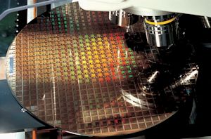
TSMC’s Version of EMIB is ‘LSI’: Currently in Pre-Qualification
Whilst process node technologies and Moore’s Law are slowing down, manufacturers and chip designers are looking to new creative solutions to further enable device and performance scaling. Advanced packaging...
19 by Andrei Frumusanu on 8/25/2020
TSMC Teases 12-High 3D Stacked Silicon: SoIC Goes Extreme
I’ve maintained for a couple of years now that the future battleground when it comes to next-generation silicon is going to be in the interconnect – implicitly this relies...
15 by Dr. Ian Cutress on 8/25/2020
TSMC Details 3nm Process Technology: Full Node Scaling for 2H22 Volume Production
At TSMC’s annual Technology Symposium, the Taiwanese semiconductor manufacturer detailed characteristics of its future 3nm process node as well as laying out a roadmap for 5nm successors in the...
58 by Andrei Frumusanu on 8/24/2020TSMC Confirms Halt to Huawei Shipments In September
TSMC on Thursday has confirmed that it had stopped processing new orders from Huawei back on May 15th. The news is the first official statement from the company on...
73 by Andrei Frumusanu on 7/17/2020
AMD Succeeds in its 25x20 Goal: Renoir Crosses the Line in 2020
One of the stories bubbling away in the background of the industry is the AMD self-imposed ‘25x20’ goal. Starting with performance in 2014, AMD committed to itself, to customers...
83 by Dr. Ian Cutress on 6/25/2020


