Intel’s Silvermont Architecture Revealed: Getting Serious About Mobile
by Anand Lal Shimpi on May 6, 2013 1:00 PM EST- Posted in
- CPUs
- Intel
- Silvermont
- SoCs
Sensible Scaling: OoO Atom Remains Dual-Issue
The architectural progression from Apple, ARM and Qualcomm have all been towards wider, out-of-order cores, to varying degrees. With Swift and Krait, Apple and Qualcomm both went wider. From Cortex A8 to A9 ARM went OoO and then from A9 to A15 ARM introduced a significantly wider architecture. Intel bucks the trend a bit by keeping the overall machine width unchanged with Silvermont. This is still a 2-wide architecture.
At the risk of oversimplifying the decision here, Intel had to weigh die area, power consumption as well as the risk of making Atom too good when it made the decision to keep Silvermont’s design width the same as Bonnell. A wider front end would require a wider execution engine, and Intel believed it didn’t need to go that far (yet) in order to deliver really good performance.
Keeping in mind that Intel’s Bonnell core is already faster than ARM’s Cortex A9 and Qualcomm’s Krait 200, if Intel could get significant gains out of Silvermont without going wider - why not? And that’s exactly what’s happened here.
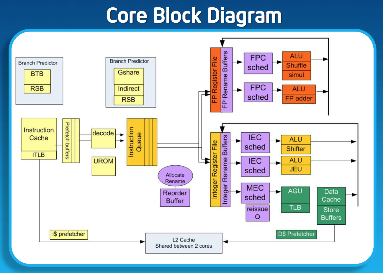
If I had to describe Intel’s design philosophy with Silvermont it would be sensible scaling. We’ve seen this from Apple with Swift, and from Qualcomm with the Krait 200 to Krait 300 transition. Remember the design rule put in place back with the original Atom: for every 2% increase in performance, the Atom architects could at most increase power by 1%. In other words, performance can go up, but performance per watt cannot go down. Silvermont maintains that design philosophy, and I think I have some idea of how.
Previous versions of Atom used Hyper Threading to get good utilization of execution resources. Hyper Threading had a power penalty associated with it, but the performance uplift was enough to justify it. At 22nm, Intel had enough die area (thanks to transistor scaling) to just add in more cores rather than rely on HT for better threaded performance so Hyper Threading was out. The power savings Intel got from getting rid of Hyper Threading were then allocated to making Silvermont an out-of-order design, which in turn helped drive up efficient use of the execution resources without HT. It turns out that at 22nm the die area Intel would’ve spent on enabling HT was roughly the same as Silvermont’s re-order buffer and OoO logic, so there wasn’t even an area penalty for the move.
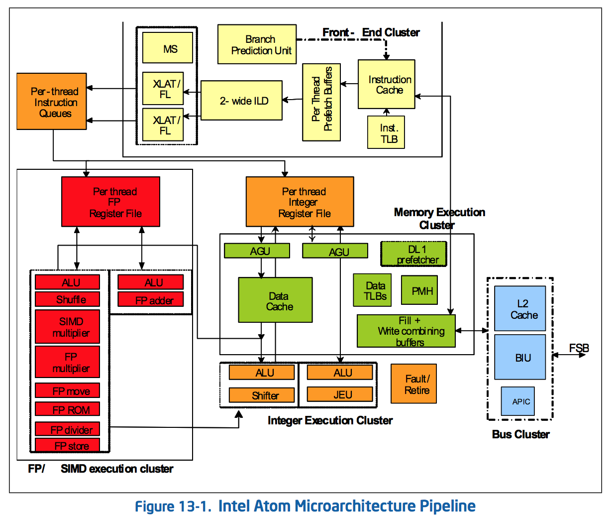
The Original Atom microarchitecture
Remaining a 2-wide architecture is a bit misleading as the combination of the x86 ISA and treating many x86 ops as single operations down the pipe made Atom physically wider than its block diagram would otherwise lead you to believe. Remember that with the first version of Atom, Intel enabled the treatment of load-op-store and load-op-execute instructions as single operations post decode. Instead of these instruction combinations decoding into multiple micro-ops, they are handled like single operations throughout the entire pipeline. This continues to be true in Silvermont, so the advantage remains (it also helps explain why Intel’s 2-wide architecture can deliver comparable IPC to ARM’s 3-wide Cortex A15).
While Silvermont still only has two x86 decoders at the front end of the pipeline, the decoders are more capable. While many x86 instructions will decode directly into a single micro-op, some more complex instructions require microcode assist and can’t go through the simple decode paths. With Silvermont, Intel beefed up the simple decoders to be able to handle more (not all) microcoded instructions.
Silvermont includes a loop stream buffer that can be used to clock gate fetch and decode logic in the event that the processor detects it’s executing the same instructions in a loop.
Execution
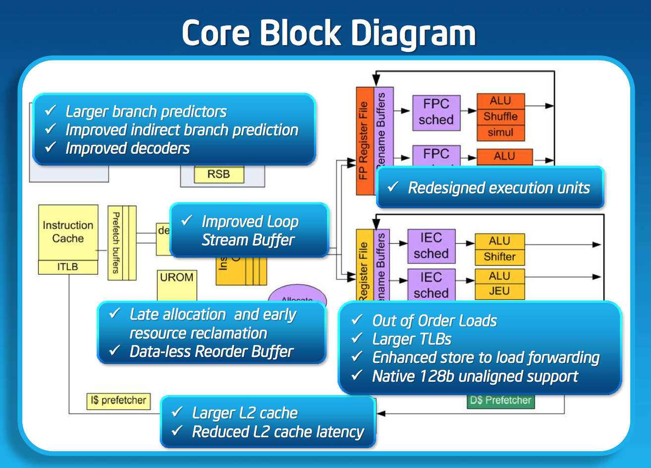
Silvermont’s execution core looks similar to Bonnell before it, but obviously now the design supports out-of-order execution. Silvermont’s execution units have been redesigned to be lower latency. Some FP operations are now quicker, as well as integer multiplies.
Loads can execute out of order. Don’t be fooled by the block diagram, Silvermont can issue one load and one store in parallel.


174 Comments
View All Comments
GTRagnarok - Monday, May 6, 2013 - link
We'll miss you :'(Pheesh - Monday, May 6, 2013 - link
I don't think the Anandtech site will miss your views and contributions. I appreciated the article and explanations for what's to come. Not everyone cares only about 'specs'.Krysto - Monday, May 6, 2013 - link
That's what I hate most about Intel's press releases, too. They are typically HIGHLY misleading, in some way or another. Remember when they made people believe the 22nm IVB would be 37% faster AND 40% more efficient? - when it was actually one OR the other, but because of the way they phrased it in the PR...and the way tech sites cloned it in their articles, that's what most people got - that they get BOTH those benefits. In the end it was HALF of each.But the worst part about it is the "churnalism" that comes after it. Since most tech sites are either too ignorant or too lazy, they just rewrite what Intel said in the PR - no questions asked.
Please remember EXACTLY what Intel says Silvermont is capable of - and I PROMISE you when this chip gets reviewed, it won't even seem close, and if you remember everything, you'll be disappointed.
Khato - Monday, May 6, 2013 - link
Actually, I don't recall where Intel stating that IVB would be 37% faster AND 40% more efficient. I believe you're confusing technical information regarding the 22nm process capabilities with a product using that process... and incorrectly interpreting that process information to boot.Homeles - Monday, May 6, 2013 - link
The only thing that I can think of is the chart comparing voltage and gate delay on the first page of this article, which was circulating a lot before the launch of Ivy Bridge. There's nothing misleading about it though, unless you don't know how to read the chart.Homeles - Monday, May 6, 2013 - link
"That's what I hate most about Intel's press releases, too. They are typically HIGHLY misleading, in some way or another."Intel, AMD and Nvidia are all guilty of this, and you know it.
t.s. - Tuesday, May 7, 2013 - link
Exactly! Hate it. It looks like all of them have an inferiority complex. They have to boast. Not confident enough with their true offerings.AssBall - Monday, May 6, 2013 - link
You know I have been coming here for 15 years and thought exactly the same thing. This article is the worst. Terrible PowerPoint graphs and gibberish. No real information. Kind of a sadness.VivekGowri - Monday, May 6, 2013 - link
The "PowerPoint" graph actually came from Excel, but it came from an article from earlier this year: http://www.anandtech.com/show/6536/arm-vs-x86-the-... (see page 3). And I dare you to find a more thorough or more comprehensively researched and tested article on SoC power consumption literally anywhere else.AssBall - Tuesday, May 7, 2013 - link
I dared, "literally", but couldn't find much. Sue us for asking for better standards.