Intel’s Silvermont Architecture Revealed: Getting Serious About Mobile
by Anand Lal Shimpi on May 6, 2013 1:00 PM EST- Posted in
- CPUs
- Intel
- Silvermont
- SoCs
Sensible Scaling: OoO Atom Remains Dual-Issue
The architectural progression from Apple, ARM and Qualcomm have all been towards wider, out-of-order cores, to varying degrees. With Swift and Krait, Apple and Qualcomm both went wider. From Cortex A8 to A9 ARM went OoO and then from A9 to A15 ARM introduced a significantly wider architecture. Intel bucks the trend a bit by keeping the overall machine width unchanged with Silvermont. This is still a 2-wide architecture.
At the risk of oversimplifying the decision here, Intel had to weigh die area, power consumption as well as the risk of making Atom too good when it made the decision to keep Silvermont’s design width the same as Bonnell. A wider front end would require a wider execution engine, and Intel believed it didn’t need to go that far (yet) in order to deliver really good performance.
Keeping in mind that Intel’s Bonnell core is already faster than ARM’s Cortex A9 and Qualcomm’s Krait 200, if Intel could get significant gains out of Silvermont without going wider - why not? And that’s exactly what’s happened here.
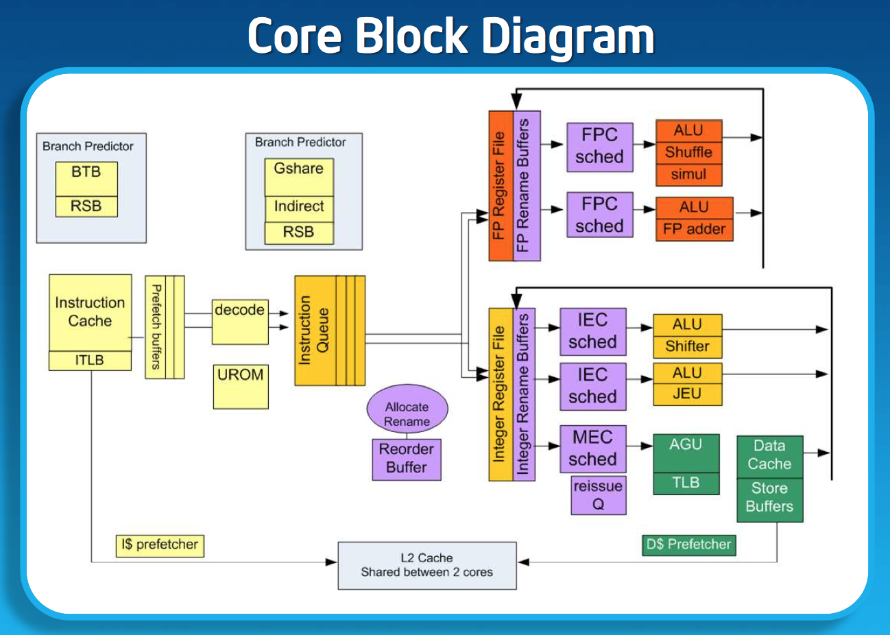
If I had to describe Intel’s design philosophy with Silvermont it would be sensible scaling. We’ve seen this from Apple with Swift, and from Qualcomm with the Krait 200 to Krait 300 transition. Remember the design rule put in place back with the original Atom: for every 2% increase in performance, the Atom architects could at most increase power by 1%. In other words, performance can go up, but performance per watt cannot go down. Silvermont maintains that design philosophy, and I think I have some idea of how.
Previous versions of Atom used Hyper Threading to get good utilization of execution resources. Hyper Threading had a power penalty associated with it, but the performance uplift was enough to justify it. At 22nm, Intel had enough die area (thanks to transistor scaling) to just add in more cores rather than rely on HT for better threaded performance so Hyper Threading was out. The power savings Intel got from getting rid of Hyper Threading were then allocated to making Silvermont an out-of-order design, which in turn helped drive up efficient use of the execution resources without HT. It turns out that at 22nm the die area Intel would’ve spent on enabling HT was roughly the same as Silvermont’s re-order buffer and OoO logic, so there wasn’t even an area penalty for the move.
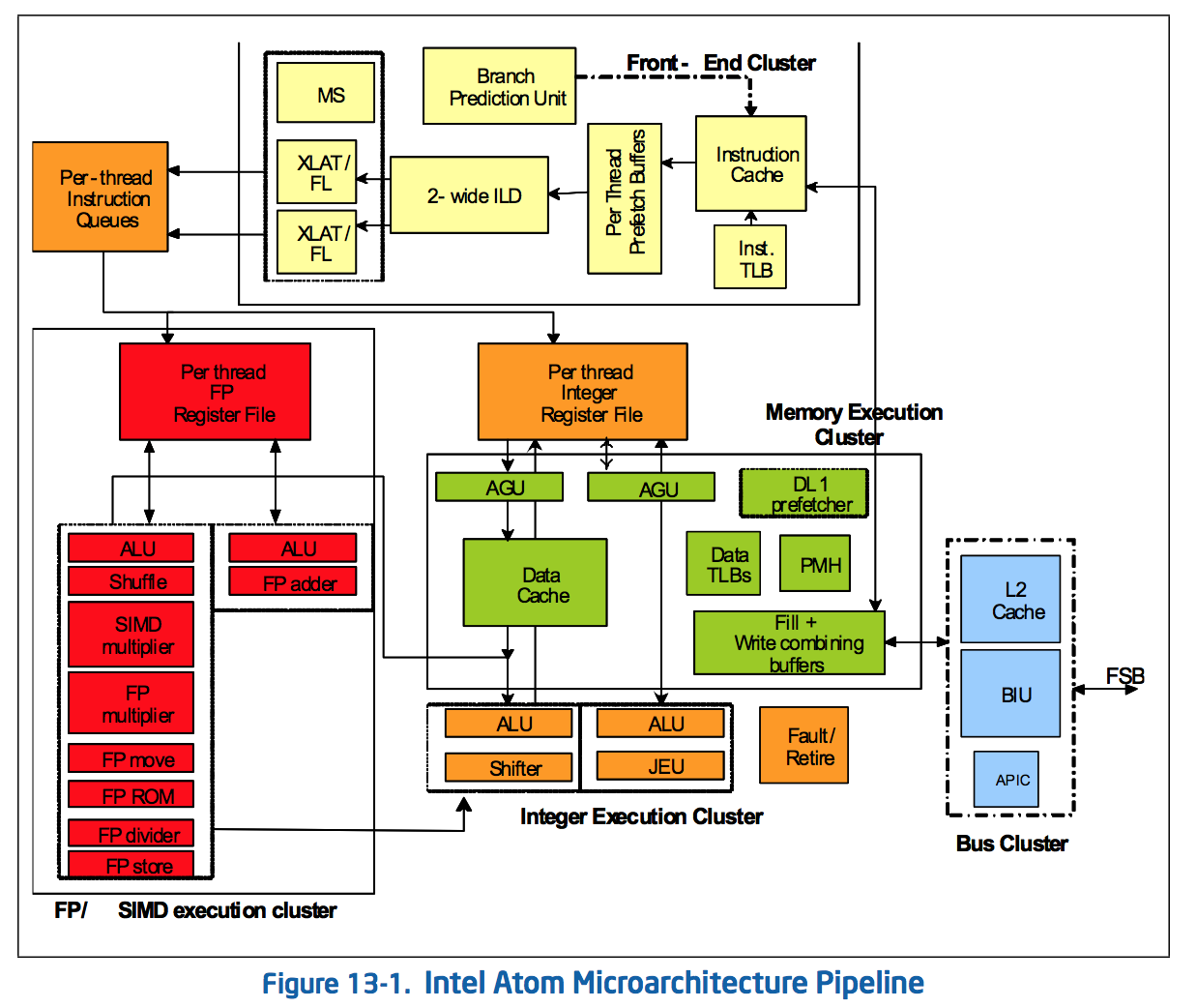
The Original Atom microarchitecture
Remaining a 2-wide architecture is a bit misleading as the combination of the x86 ISA and treating many x86 ops as single operations down the pipe made Atom physically wider than its block diagram would otherwise lead you to believe. Remember that with the first version of Atom, Intel enabled the treatment of load-op-store and load-op-execute instructions as single operations post decode. Instead of these instruction combinations decoding into multiple micro-ops, they are handled like single operations throughout the entire pipeline. This continues to be true in Silvermont, so the advantage remains (it also helps explain why Intel’s 2-wide architecture can deliver comparable IPC to ARM’s 3-wide Cortex A15).
While Silvermont still only has two x86 decoders at the front end of the pipeline, the decoders are more capable. While many x86 instructions will decode directly into a single micro-op, some more complex instructions require microcode assist and can’t go through the simple decode paths. With Silvermont, Intel beefed up the simple decoders to be able to handle more (not all) microcoded instructions.
Silvermont includes a loop stream buffer that can be used to clock gate fetch and decode logic in the event that the processor detects it’s executing the same instructions in a loop.
Execution
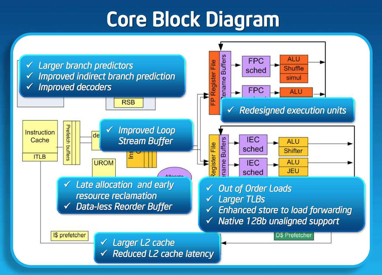
Silvermont’s execution core looks similar to Bonnell before it, but obviously now the design supports out-of-order execution. Silvermont’s execution units have been redesigned to be lower latency. Some FP operations are now quicker, as well as integer multiplies.
Loads can execute out of order. Don’t be fooled by the block diagram, Silvermont can issue one load and one store in parallel.


174 Comments
View All Comments
silverblue - Monday, May 6, 2013 - link
I do wonder how much having a dual channel memory interface helps Silvermont, though. It's something that neither Atom nor Bobcat has enjoyed previously, and I've not heard much about Jaguar on this subject (ignoring the PS4, that is). AMD certainly has the lead on ISAs though, so regardless of how good Silvermont is, it's going to trail in some places.I'm a little confused as to the virtual lack of a comparison to AMD in this piece; yes, Intel did say they wanted to beat ARM at its own game, but with Jaguar-powered devices already in the wild and AMD sporting a new custom-CPU team for whoever wants whatever, this is going to be interesting.
Benchmarks, please! ;)
powerarmour - Monday, May 6, 2013 - link
Atom had dual channel memory with the ION chipset btw.silverblue - Monday, May 6, 2013 - link
Really? Oh well, in that case then, maybe not too much.Spunjji - Wednesday, May 8, 2013 - link
Only until Intel murdered that, of course :|ajp_anton - Monday, May 6, 2013 - link
Where did you find "8x" in the slides?Gigaplex - Tuesday, May 7, 2013 - link
AMDs HSA is most definitely something to be enthusiastic about.theos83 - Monday, May 6, 2013 - link
You're right, I've seen this tendency in AT's reviews and discussions as well. I understand that a lot of it comes from reviewing PC components and processors where Intel dominated the market. Also, most of the slides here are marketing material. For example, the 22nm Ivy Bridge tri-gate plots have been out since 2011. True, Intel is the first and only foundry to bring FinFETs to the market successfully and I applaud them for that. However, the performance vs power advantage is not that evident, since even though Tri-gates allow 100mV reduction in threshold voltage and hence, supply voltage, various blogs have reported that most Ivy bridge processors did not scale down supply voltage below 0.9V. FinFETs are great for high performance parts, however, you need to really pay attention to reliability and variation to make it successful for SoCs, they are a completely different ball-game.Also, the rest of the SoC makers already have roadmaps ready for the future, they are a fast moving target. Hence lets see benchmarked numbers from Intel processors before jumping on the marketing bandwagon.
Pheesh - Monday, May 6, 2013 - link
"However, the performance vs power advantage is not that evident, since even though Tri-gates allow 100mV reduction in threshold voltage and hence, supply voltage, various blogs have reported that most Ivy bridge processors did not scale down supply voltage below 0.9V." Didn't the start of the article cover that they are using a different manufacturing process for these lower power SOC's as compared to ivy bridge processors?saurabhr8here - Monday, May 6, 2013 - link
The SoC process has some differences in the metal stack for higher density and has additional transistor flavors (longer channel lengths). Check Intel's IEDM 2012 paper for more information, however, the truth is that their tri-gate process improvements claimed in the 'plots' shown and actual performance improvements in processors have a significant gap. I think that Intel tri-gates are great, but they aren't as 'wonderful' as presented in the marketing slides.Krysto - Monday, May 6, 2013 - link
Thank You! People are starting to get it.