A Look at Altera's OpenCL SDK for FPGAs
by Rahul Garg on October 9, 2013 8:00 AM ESTAltera's OpenCL Implementation Details
We go over how OpenCL kernels are compiled to FPGAs, and discuss some of the unique advantages of Altera's implementation over, say, GPUs.
Kernel compilation
Before getting into FPGAs, let us first look at how OpenCL kernels are compiled to GPUs. I am going to oversimplify things here so the discussion is not totally accurate, and details vary considerably across GPUs, but the objective is to give you a good idea of the concepts.
Every GPU has its own instruction set. Each vendor's OpenCL compiler compiles OpenCL to the native instruction set of the GPU being targeted. OpenCL work-groups typically get mapped to a compute unit in a GPU, and each compute unit can run many workgroups in parallel. Each compute unit has a fixed number of resources such as number of registers and local memory that get divided between the workgroups. Thus, the number of work-groups that can run in parallel depends upon the resources required to run one workgroup. Very approximately, arithmetic operations of work-items within a work-group get mapped to ALUs within a compute unit. If there are 64 ALUs in a particular compute unit, then arithmetic instructions from 64 work-items are processed at once by each compute unit.
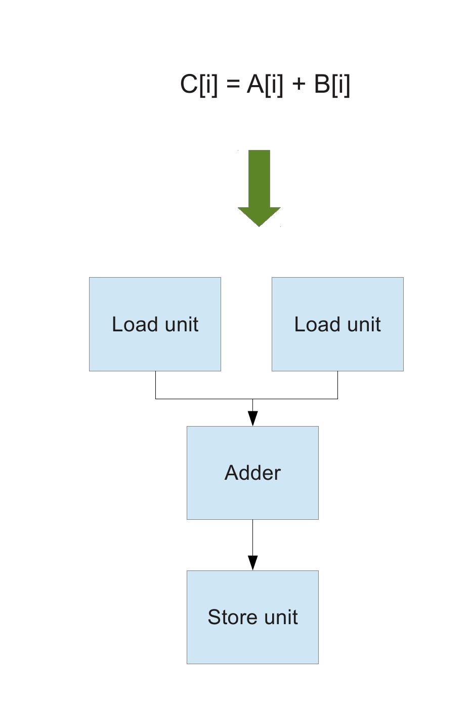
Now let us look at Altera's OpenCL compiler. Altera's OpenCL compiler reconfigures the FPGA so that it becomes a custom processor designed for computing your kernel. For example, in our vector add example, each work-item does 2 loads (one from vector A, one from vector B), one floating-point add and one store (vector C). Then, Altera's compiler will generate 2 load units, 1 adder and 1 store unit.
Behind the scenes, Altera's compiler is currently generating Verilog but this is an implementation detail that can change, and the programmer doesn't need to concern herself with it. As discussed earlier, Altera's OpenCL implementation tries to be smart and tries to avoid generating any unnecessary units. For example, if your kernel does not use floating point arithmetic, then no floating-point logic is generated. Further, let us say your kernel has operations such as (a*b*c + d*e). Such operations would map to multiple instructions in a CPU or a GPU but in an FPGA, the compiler may generate an ALU that performs this operation in a single step.
One potential weakness of FPGAs is that the compilation of OpenCL kernels to FPGAs can take time and so Altera primarily provides an offline compiler. Compiling OpenCL kernels for CPUs or GPUs typically happens in the order of hundreds of milliseconds to seconds on most modern machines. However, compilation time for FPGAs can be significantly longer and can often be in hours instead of seconds.
UPDATE: See comment from Kishonti (makers of tools like CLBenchmark, which we use ourselves for GPGPU testing) where they say that the compile time was indeed in hours for their tests. I can see that this can be an issue. On CPUs and GPUs, we are used to fast compile times which allows for quick iterations of testing and tuning kernels. On FPGAs, the development time can be longer due to compilation time bottleneck.
Mapping parallelism: Pipelining and resource replication
Another interesting aspect is how OpenCL's parallelism is mapped to an FPGA. In computer architecture, you can obtain parallelism in at least two ways: (a) Resource replication, obtained by replication of the same resource (such as a CPU core or a GPU compute unit) multiple times (b) pipeline parallelism, which relies on different types of functional units acting in parallel on different steps. For example, load/store units may act in parallel with ALUs.
Altera's SDK takes advantage of pipelining as well as resource replication. First we look into pipelining. Consider our vector addition example. It consists of 3 steps: load, add and store and Altera's SDK will generate a 3-stage pipeline. At any given time, upto 3 different work-items will be active in the pipeline in parallel. When work-item N is executing the store stage, work-item N+1 is executing the add stage, and work-item N+2 is executing the load. We show an example below:

Our example consists of a very simple problem and upto 3 work-items were executing in parallel in the pipeline. For more complex kernels, Altera's SDK will generate much deeper pipelines with many more work-items active in the pipeline at the same time. In a general purpose processor, the number of various functional units, such as ALUs and load/store units, as well as the functionality of each unit and the connection structure between these units is fixed at design time of the processor. This fixed structure may not be optimal for all applications. However, in an FPGA the pipeline structure and the number and types of functional units present is customized to suit your application.
If the pipeline generated for your application is simple and does not eat all the resources on the FPGA, then you can instruct Altera's SDK to also attempt to create multiple copies of the pipeline. However, instead of outright replication of the pipeline, in many cases a better option is to merge multiple work-items and effectively vectorize a problem. For example, in our kernel, we can modify the kernel so that each work-item computes a vector of 8 elements. Vectorization is somewhat more efficient but not always applicable. Altera's SDK allows you to control whether you want to vectorize or replicate your pipeline.
To summarize, Altera's SDK places pipeline parallelism at the forefront and can generate deep, application-specific pipelines. Resource replication is controlled by the programmer and depending on the problem can be done either by implementing a wider pipeline through vectorization or through outright pipeline replication.
Local memory
Next, we look at local memory. On GPUs, local memory is typically implemented using on-chip SRAM. On GPUs, this SRAM has a fixed size and a fixed number of banks, with each bank typically returning 1 or 2 results every clock cycle. For example, some GPUs provide 32kB of local memory per SMX and this is divided into 32 banks. Thus, on a GPU, the number of read/write ports to/from the on-chip SRAM is fixed. However, on an FPGA, the size and configuration of the local memory can be customized. One kernel may require a "deeper" local memory with fewer read/write ports, while another kernel may require a wider local memory with larger number of read/write ports. Thus, in addition to customized units and a custom pipeline, on an FPGA the local memory is also customized to your kernel. As mentioned in the previous section, compared to current GPUs FPGAs have relatively large amount of memory that can be used as local memory.
High speed I/O to external devices
One of the bottlenecks in many high performance applications is that the data to be processed comes from an external I/O device. For example, input data might be a large file read from an SSD, or streaming data from a video camera, or data from network port. Traditionally this data was transferred to a buffer in system RAM by the external I/O device, and then copied by the CPU to another temporary buffer in system RAM and finally copied to the accelerator/co-processor over PCIe. Obviously, this multiple copying of data is wasteful and can be a big bottleneck.
FPGAs can communicate to external world (PCIe, network connections, storage devices etc.) through transceivers. Different FPGA products have different number of transceivers with different datarates. Currently, the most impressive offering from Altera is the Stratix V GX with upto 66 14.1 Gbps (bidirectional) transceivers. The number of transceivers actually exposed by a given FPGA board depends upon both the FPGA used as well as the board design. Connecting an external I/O device may require additional logic and Altera and partners will readily sell you solutions for a number of standard interfaces. The high bandwidth I/O makes the FPGA ideal for streaming/filtering type applications.
Unfortunately, the OpenCL standard does not really cover this type of scenario well and so Altera is working on providing custom extensions to OpenCL that allow you to use external I/O devices as inputs or outputs of OpenCL kernels for streaming applications. Altera tells me this is similar to the pipes functionality introduced in the provisional OpenCL 2.0 spec.
It is worth mentioning that Nvidia provides a competing solution called GPUDirect for CUDA. As of CUDA 5.0, it is possible for external I/O devices such as other Nvidia GPUs, SSDs and network cards to read/write the GPU memory directly over PCIe bus without going through the host. However, the net bandwidth is limited to PCIe 3.0 x16 currently, which works out to about 16 GB/s in each direction which is much lower than the peak theoretically obtainable on, say, the Stratix V GX FPGA (~116 GB/s in each direction). In practice, Nvidia's GPUDirect solution is sufficient for many applications but there are definitely some applications where the FPGA's bandwidth advantage will be extremely important. Another limitation of Nvidia's GPUDirect is that it is currently only available in CUDA and not in OpenCL.


56 Comments
View All Comments
MrSpadge - Wednesday, October 9, 2013 - link
BTW 2: David, you might want to contact Slicker, the admin of Collatz@Home. His project is fairly simple (and not that useful.. but people like it nevertheless) and has regularly been at the forefront of new technology (CUDA, ATI Stream, OpenCL, Intel GPUs..). Usually he's also very responsive. I could imagine a deal like: you give him access to your hardware, and if he succeeds you could get loads of publicity (attracting buyers and further developers) and quite a few sales.viv32 - Wednesday, October 9, 2013 - link
Application driven reconfigurable hardware is an exciting idea. I am not sure how dense the fpga should be to support the complexity of today's GPUs (If they want FPGAs to replace GPU ASICs). We design network processors and our fpga emulation boards need atleast 4 Stratixs for complete emulation. If the FPGA gate count can match the GPU then can they still be cost effective? My2c .. please correct me if I'm wrong (I'm no FPGA jockey).rahulgarg - Wednesday, October 9, 2013 - link
Well it depends. The objective in this case isn't to emulate the GPU at all. If the GPU is actually already a very good fit for your application, then going to FGPAs won't gain you much. But let us say in an application that does not use GPU's texture units, you don't really want to generate texture units on an FPGA. The idea isn't to emulate GPU's units or its pipeline, rather it is to generate a *different* pipeline that is more suitable for your application.wyx087 - Wednesday, October 9, 2013 - link
Benefit of using hardware description languages such as VHDL is just that, it describes the hardware, forcing you to think in terms of the cells gets placed down. OpenCL is a compute language, its programmers won't take into account something as simple as multipliers are very expensive in hardware unless done in powers of 2.Also, vast number of university courses do VHDL/Verilog/SystemVerilog as standard. Electronics is the course title. I have no doubt the number of HDL experts is much more than OpenCL experts on this planet.
The way around "slow compile" is simulation. I see no mention of simulation tools for designing OpenCL on FPGA. Without simulation tools, it is impossible for this to take off. Simulation is the way we verify our design on a functional level.
The "compile" (it is known as synthesis and implementation or map, place and route) time is indeed in hours for large designs. Remember you are not just generating a binary for a processor, you are generating a binary file that describes the actual hardware. Put it simply, you are generating THE processor.
- Professional VHDL programmer
loki1725 - Sunday, October 13, 2013 - link
This is actually what I was going to say. When I was an undergrad in EE (1997-2001) our embedded electronics course used VHDL. I taught in the EE department of a different university from 2009 to 2013 and we offered several courses that used VHDL. While there may not be more VHDL courses then OpenCL, the numbers are probably comparable.Still, really cool article, and anything that helps drive the adoption of FPGAs is a good step forward.
toyotabedzrock - Wednesday, October 9, 2013 - link
So the compile time happens beforehand but how long does it take for the fpga to configure itself when you run a program.rahulgarg - Wednesday, October 9, 2013 - link
Well once you have done the compilation, my understanding is that flashing the binary is actually very fast so that is not an issue.John32 - Wednesday, October 9, 2013 - link
Are you saying Altera doesn't provide a simulation stage to testing functionality? That's done before generating the binary file for all designs. Generating the binary file is the last thing you do after verifying everything works functionally.You say Altera generates Verilog code in then I assume that goes through their standard synthesis, place and route tools. I don't see why you can't do a software and "hardware" (ie. the Verilog code) co-simulation. That's what is normally done during verification. I have C/C++ code that talks to the Verilog code. The C/C++ code is compiled to a binary file and the Verilog code is compiled within an HDL simulator software. Then the entire thing is simulated together. Once that checks out, I generate the binary file and load into the FPGA. I use the same C/C++ code but now with the actual FPGA.
John32 - Wednesday, October 9, 2013 - link
Also, the whole "will it fit into the FPGA" issue is probably going to be a big problem for the likely target audience for this. You have no idea how the OpenCL code is being translated into hardware (ie. gates, LUTs, flip-flops, etc.). That all depends on your code and Altera's software to hardware algorithm.This reminds me of Xilinx's System Generator for MATLAB. It's a nice and easy way to get scientists to test their algorithms in hardware to see a ballpark figure of how fast it can be but it's definitely not the way to go for a final product.
John32 - Wednesday, October 9, 2013 - link
I guess there's also the "will it meet timing" problem. What clock speeds does Altera use? Do they just use whatever clock speed they can achieve (ie. one design clocks at 400 MHz while another can only go 100 MHz)?