The Intel Skylake Mobile and Desktop Launch, with Architecture Analysis
by Ian Cutress on September 1, 2015 11:05 PM ESTWhat to Expect
With Intel going for a full YUHS launch today, looking up and down the stack there are a number of interesting things to consider at each segment. Starting with Skylake-Y, or Core M, the new branding to m7/m5/m3 will hopefully make it easier for users to ascertain the performance of their processor, but it also allows Intel to inject vPro into various SKUs, such as the upcoming update to Intel’s Compute Stick.
In the mini-PC space, through various sources in the industry, we are told that it is the vPro moniker for these devices (such as the NUC and Compute Stick) that generate the higher proportion of sales. At this point, the vPro versions of Core M are not due out until later in Q4/even Q1, but I assume we should see something at the Consumer Electronics Show during the first week of January.
One element we haven’t touched upon is how Intel will implement different TDP aspects to both its Skylake-Y and Skylake-U lines. With Haswell and Broadwell, most processors had a cTDP Up and a cTDP Down mode that allowed the device OEM to take a processor and move it slightly outside its normal TDP window, perhaps to take advantage of a chassis design they already had and either increase battery life or increase performance.
Now due to Speed Shift, one could argue that cTDP down is less relevant, and when cTDP up is available and a Speed Shift aware operating system is installed, that setting might be used as well. Because Speed Shift is not universal, there is still this element of cTDP Up and Down to contend with. To insert a few more caveats, it seems like SDP (scenario design power) might also be part of the equation, especially in the Skylake-Y domain.
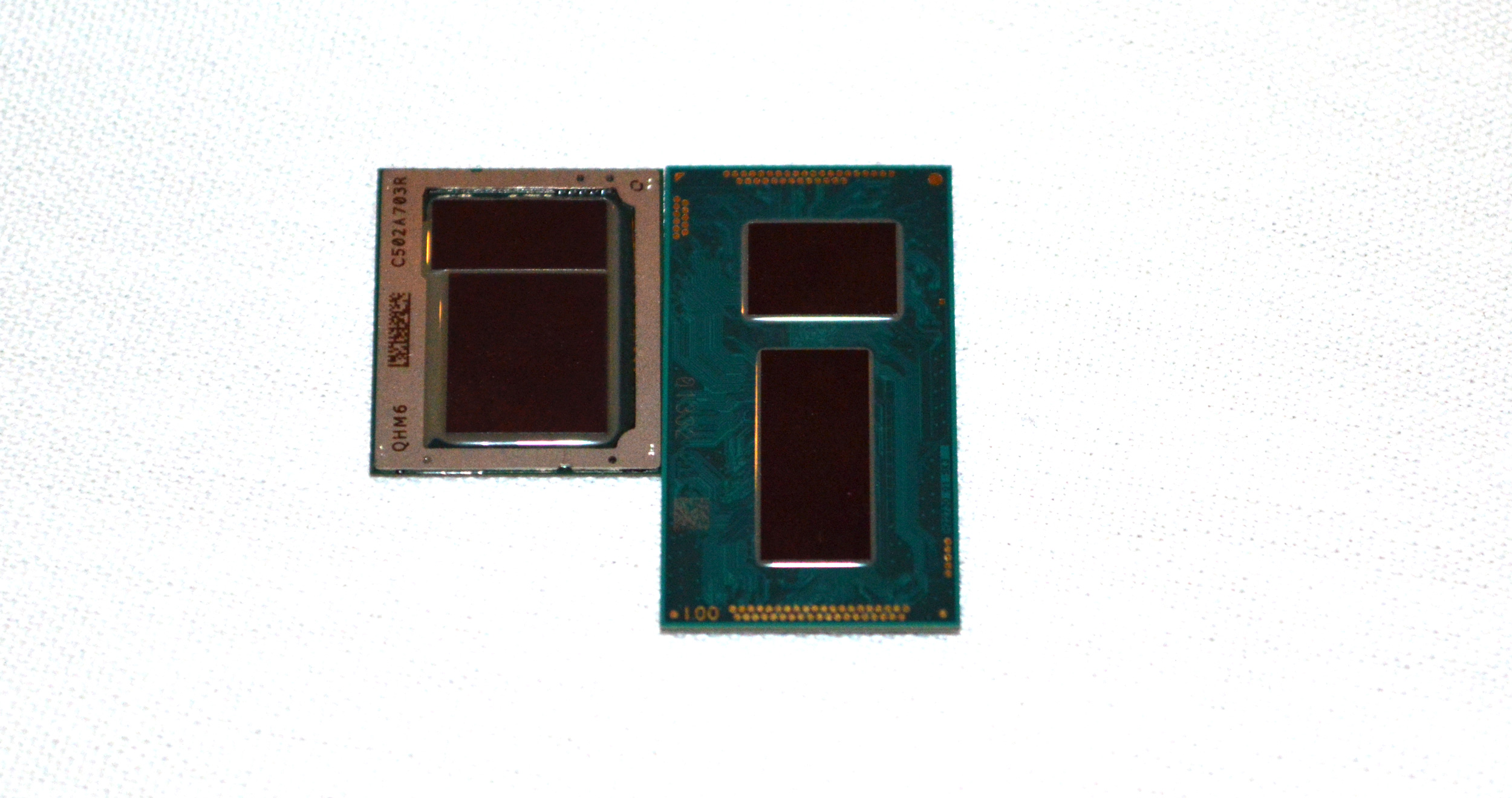
It is worth noting that the Skylake-Y package is crazy small. At IDF Intel showed off a finished Skylake-Y package to demonstrate the CPU die size in relation to the package size, and to compare the overall package size to the already small Broadwell-Y package. While both packages are still 16.5mm wide, Intel has compacted the overall layout and squared off the CPU die, bringing the height of the Skylake-Y package down from 30mm to 20mm, a 33% savings in package size.
Meanwhile Intel also had the other BGA Skylake processor packages on display as well:

Actually in this shot, we can calculate the die size of the Y 2+2 die to be approximately 98.5 mm2 (9.57mm x 10.3mm). This is compared to the 4+2 arrangement on Skylake-K which we measured at 122.4mm2. At this package size of 20 x 16.5 mm, Intel is claiming a 40% gain in graphics performance for Skylake-Y over Broadwell-Y, which will be interesting to compare when we get some samples in house.
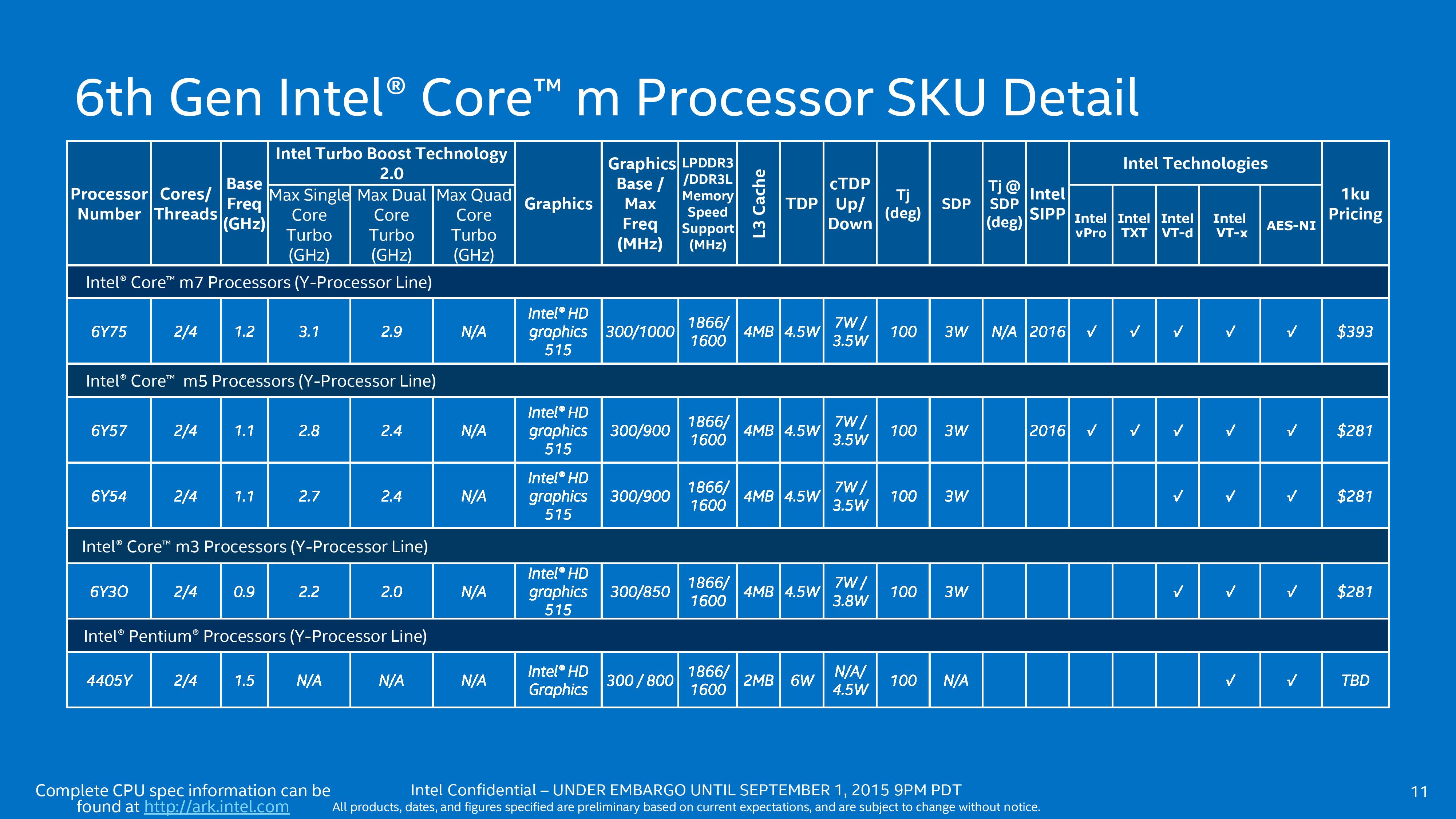
Skylake-Y still comes in as Intel’s premium low power processor, with 1K pricing from $281 to $393. That more or less aligns with Broadwell-Y, but we also get a Pentium model that is severely cut with no turbo mode and only 1 MB of L3 cache per core.
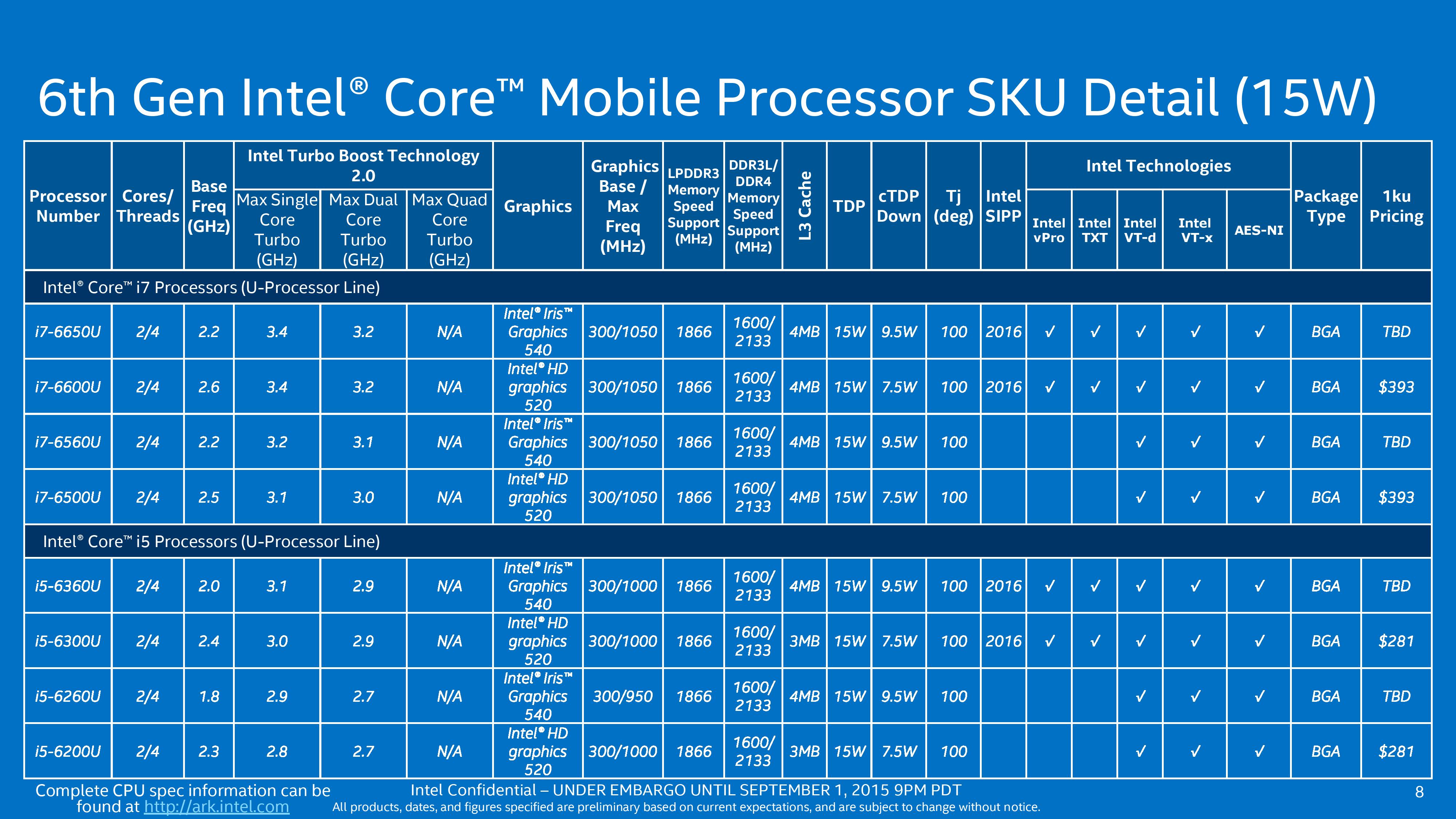
The 15W models of Skylake-U either follow the 00U naming for GT2 graphics (24 EUs) or 50U/60U for GT3e graphics (48 EUs with 64MB eDRAM). The pricing on the GT3e parts is not given as they will be coming later in the year, but it can be pointed out that the base frequency for the GT2 parts is actually higher than the GT3 parts. Also, the L3 cache on the i5-U processors with GT2 is at 1.5 MB/core rather than 2 MB/core. Normally all the i5 parts would be below the i7 parts, but because the eDRAM arrangement moves up to 2 MB/core, the i5-U parts with GT3e have to comply.
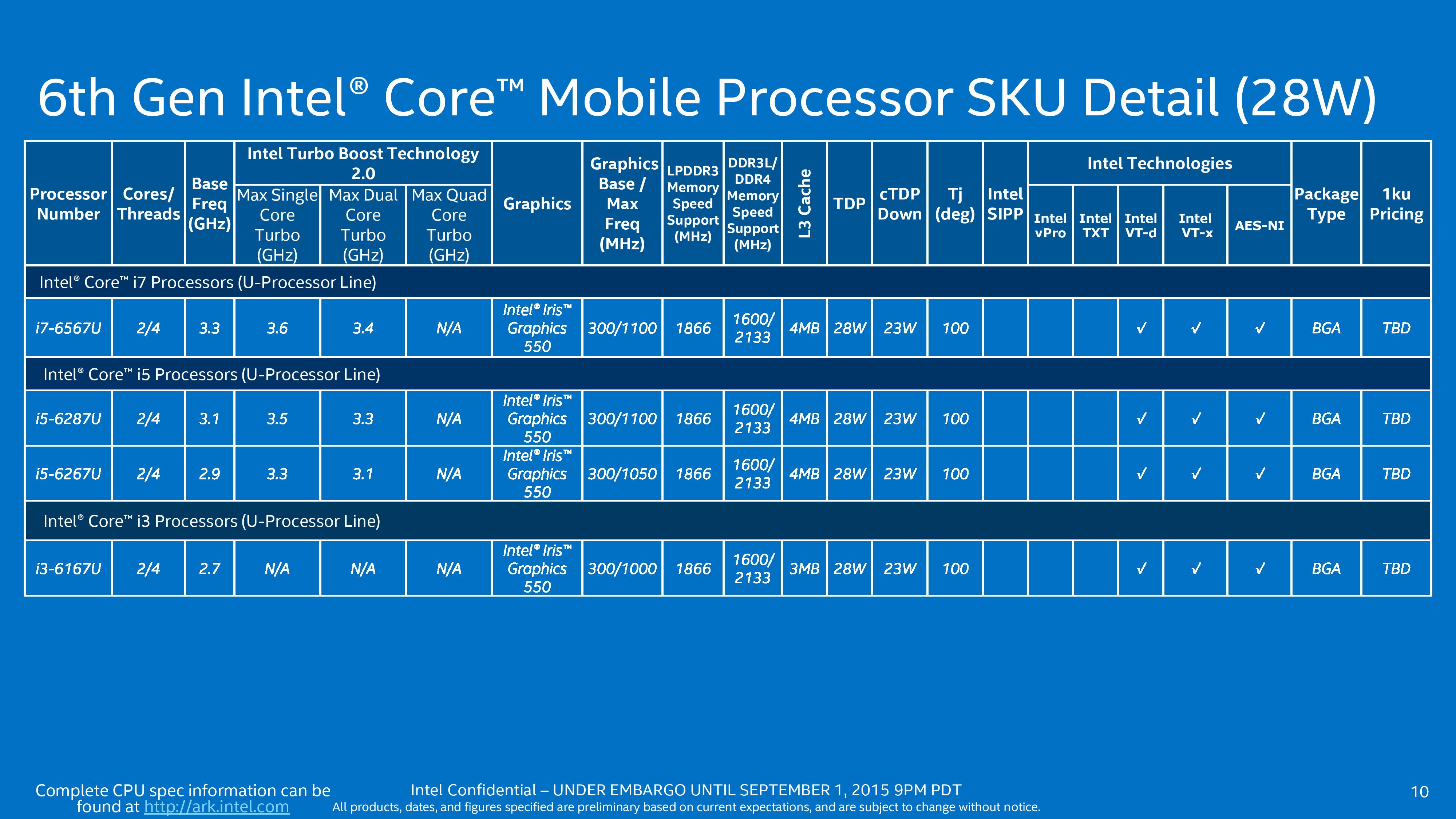
Moving up to 28W with Skylake-U presents us with the higher power GT3e models. Similarly, the pricing has not been announced for these but for all the processors the base frequency is relatively high (2.7 GHz to 3.3 GHz) with only a small jump to the maximum frequency. The i3 at the bottom without any turbo frequency but with GT3e would be an interesting part to play with.
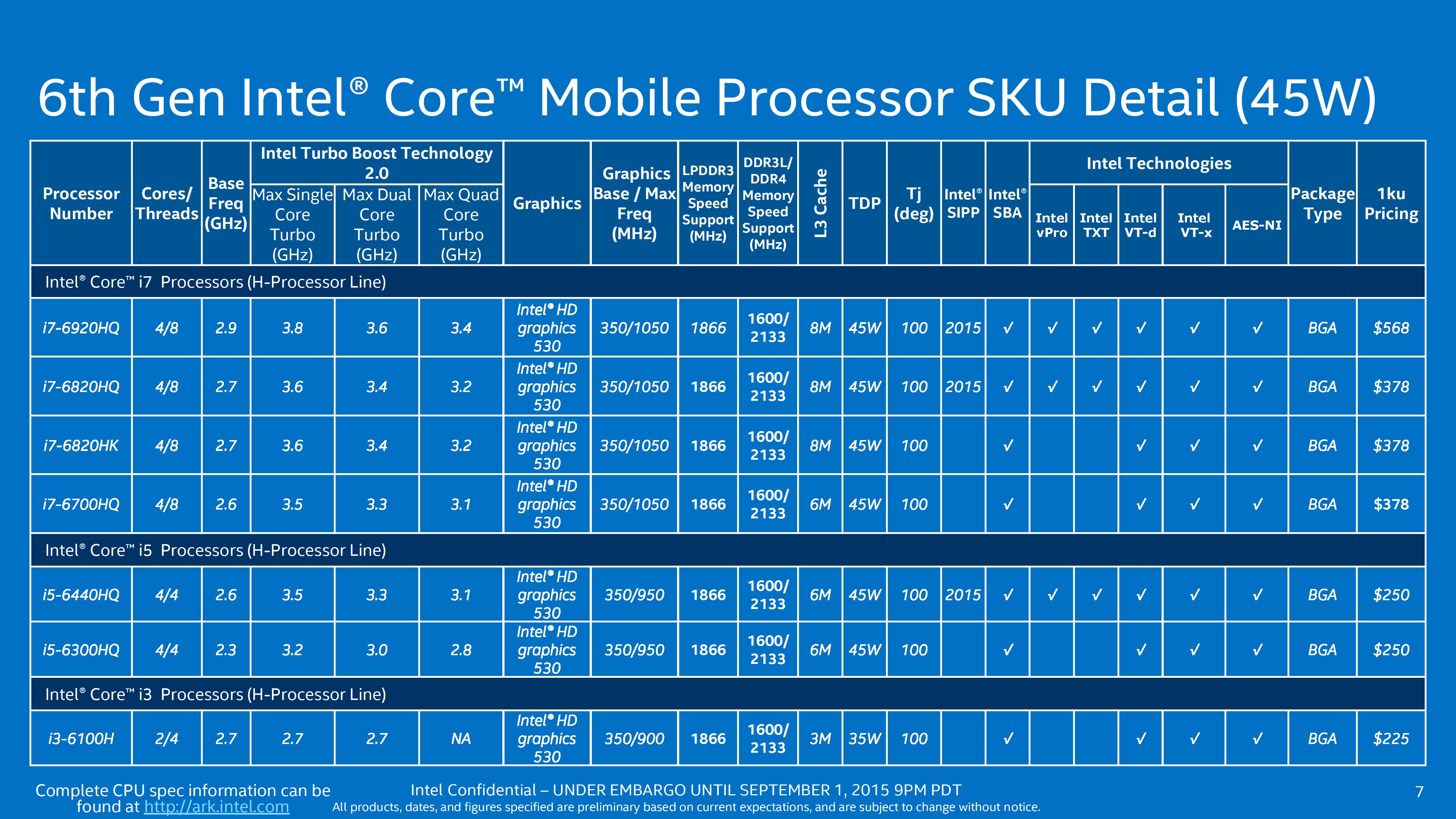
At 45W, the Skylake-H mobile processors almost all move into quad core territory here, aligning with the power increase, but also moving down to GT2 arrangements. We get a vew vPro enabled parts here too, and the pricing of the i5 seems quite reasonable.
There is one part that stands out – the i7-6820HK. This is Intel’s mobile part that can be user overclocked. Yes, that’s not a typo. This processor is designed to go into laptop systems that have sufficient cooling (either high powered air… or water) and can be pushed when they are needed. Expect to see this part in the large 17” desktop replacement gaming systems over the next few months.
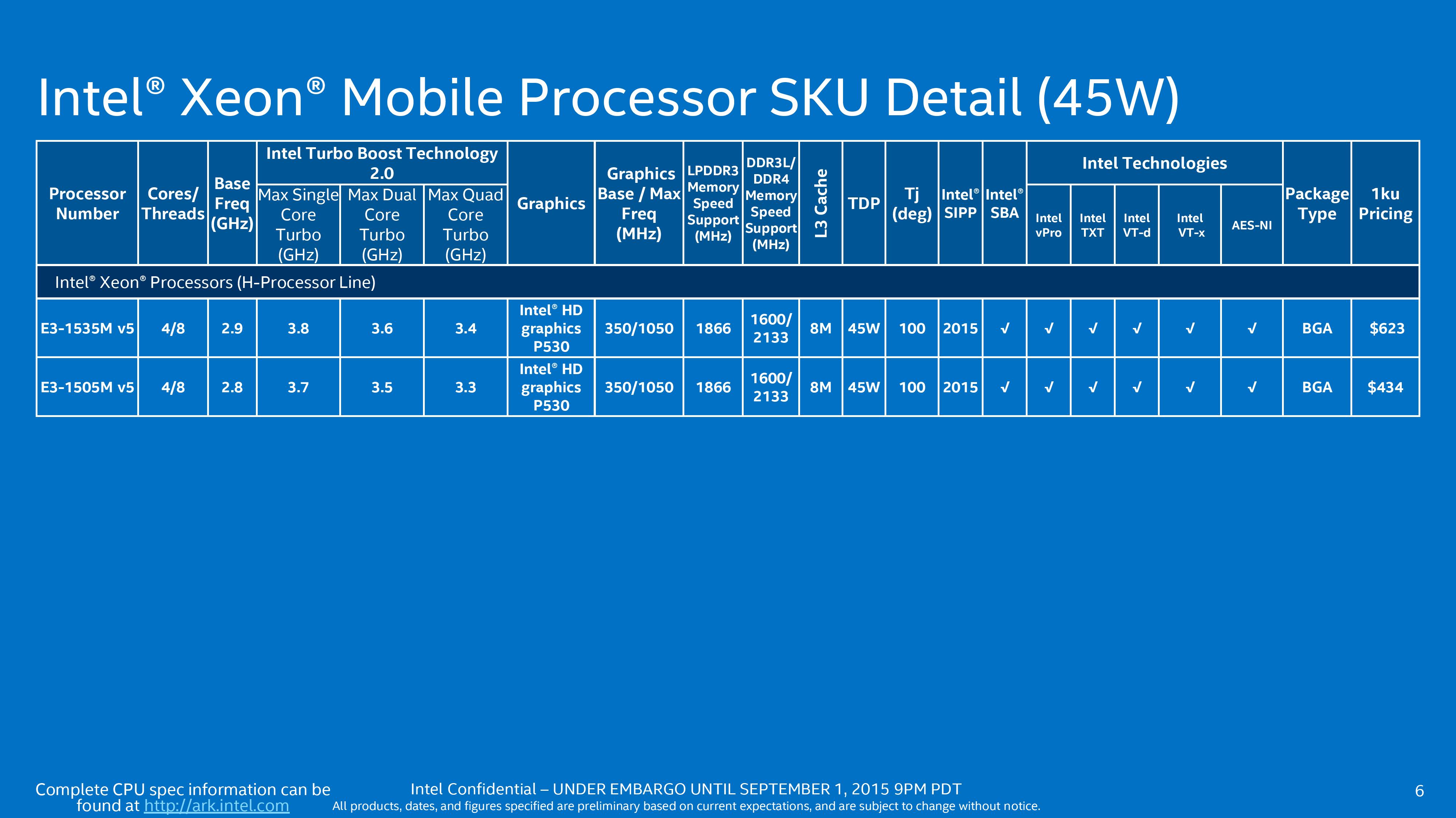
Intel is also releasing a couple of mobile processors under the Xeon branding. This means ECC support and all the other Xeon benefits, but in a processor specifically designed for notebooks rather than a repurposed desktop processor that might not fit properly / give the best ergonomics. When these were announced, it was perhaps wishful thinking that Xeon would come down to 15W, perhaps offering ultrabooks with this feature set, though I imagine at 45W we will see some desktop-replacement workstations with professional grade graphics cards, such as the already-announced Lenovo workstation laptops.
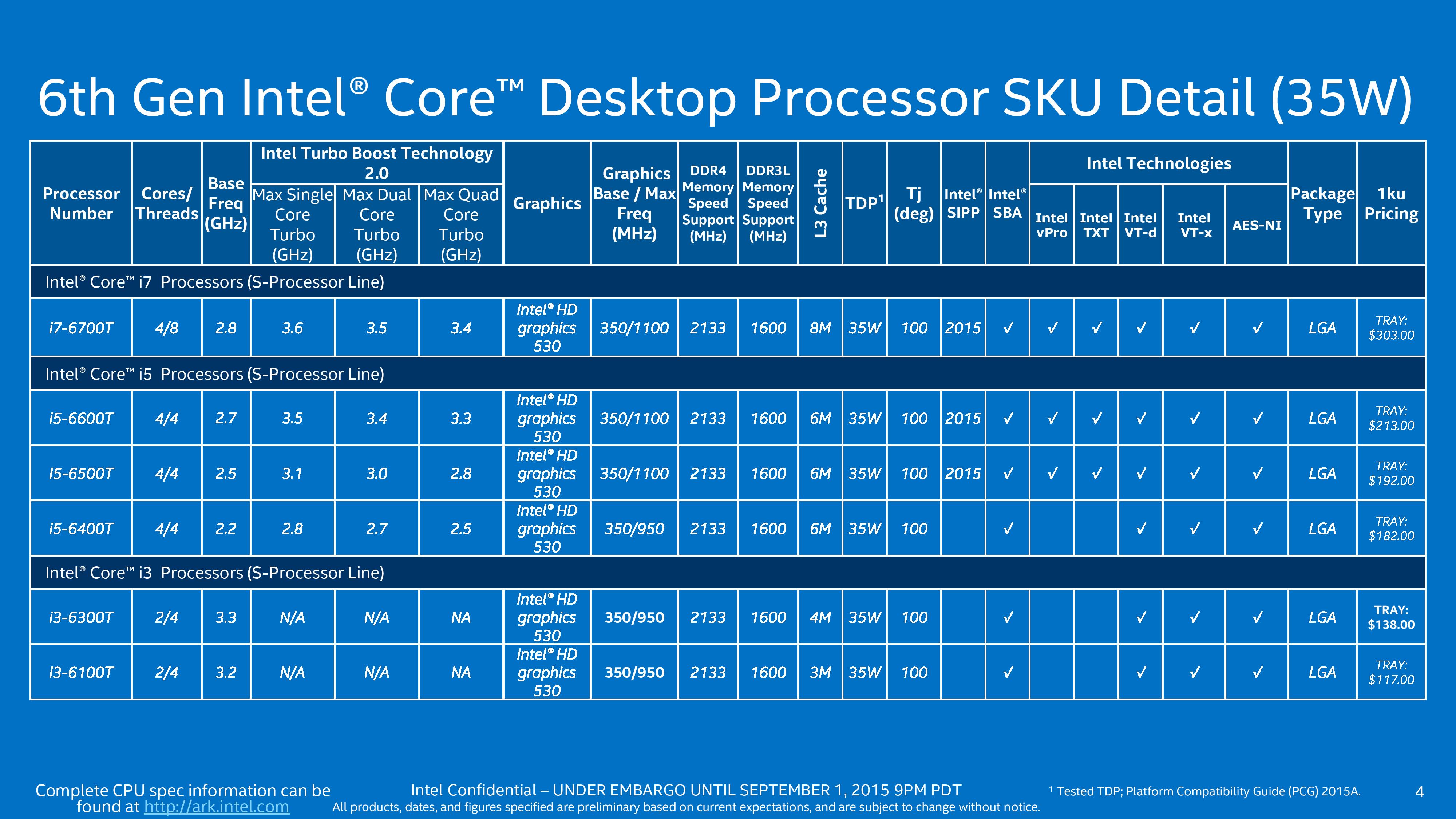
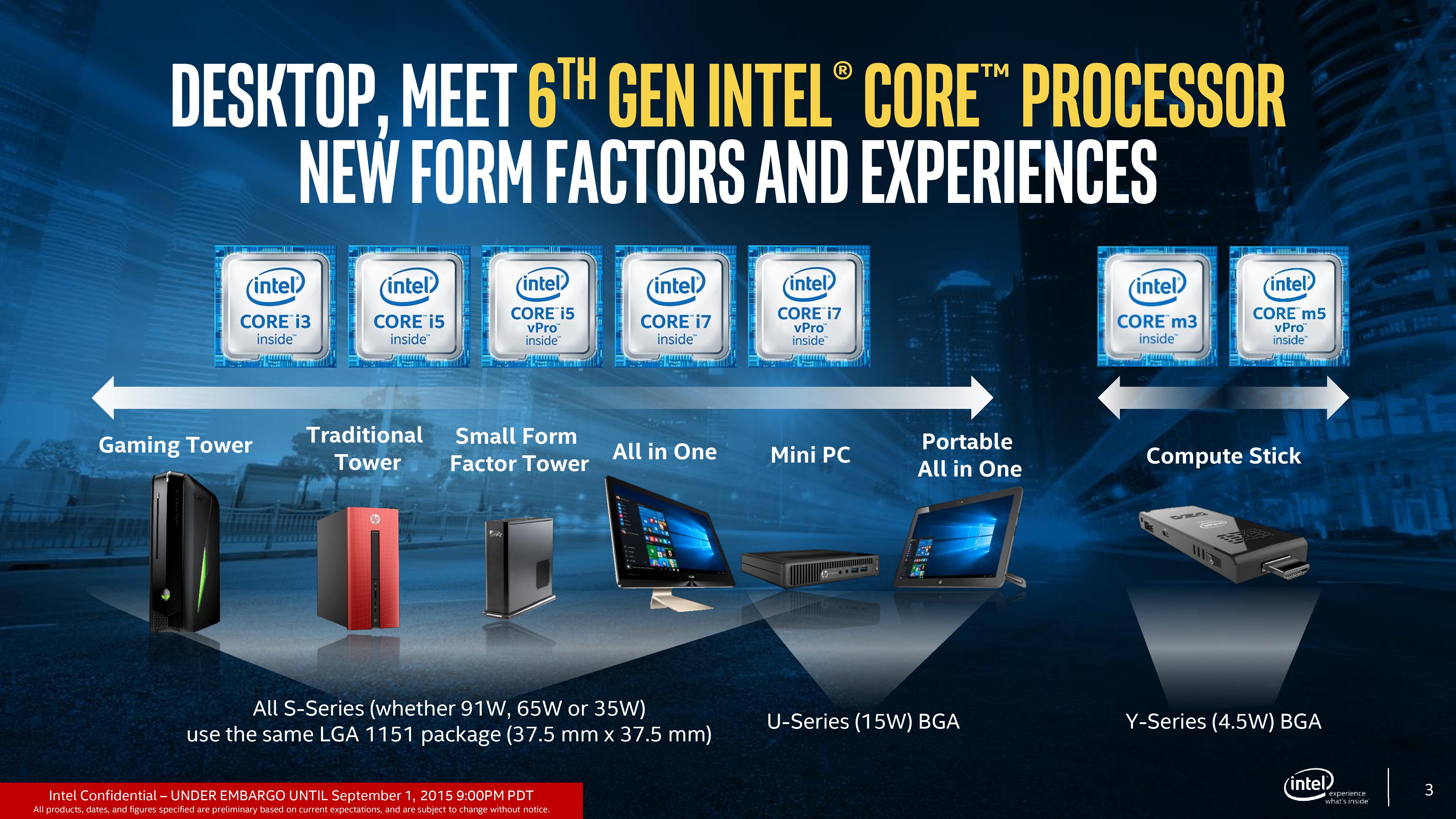
On the Skylake-S side of the equation, the processors come in two segments. Here is the list of the low powered processors that have the ‘T’ in the name, or unofficially known as ‘Skylake-T’. These are all 35W, some with vPro, but covering the i3/i5/i7 lines sufficiently.

The non-T and non-K desktop processors come in at 65W, and there are no real surprises here in the product lines as they migrate well enough from previous generation designations. All the Skylake-S i3/i5/i7 processors have HD 530 graphics.
Beyond Skylake and to Kaby Lake
Post Skylake, Intel is breaking from the tick-model to tick-tock-tock, posting a third generation on 14nm called Kaby Lake (pronounced Kah-bee, as far as we were told).
This stems from the issues of moving to smaller process nodes. At 14nm, this equates to only 90 silicon atoms, meaning ever more intensive manufacturing is required which drives up cost and reduces yield. Due to the issues Intel had at 14nm using their second generation FinFET method and more advanced double patterning, initial costs were high and yields were lower than expected for the timeframe, pushing Broadwell to a later-than-expected timeline. Skylake was kept to the regular timeline, resulting in a brief outing for Broadwell (on the desktop especially). But we suspect that similar reasoning is behind a delay from 14nm to 10nm –more esoteric ways under conventional methodology are required to keep driving the node down, and with that comes extra challenges that delay both time to market and yield numbers before tweaking the design.
We’ve mentioned in the past that the development of extreme-ultra-violet (EUV) technology is one element that could assist this drive down, however Intel is not expected to implement this for 10nm but rather for 7nm, which is still several years down the road. To that end, tick-tock is not dead, but merely stretching out.


173 Comments
View All Comments
prisonerX - Thursday, September 3, 2015 - link
You can't make a purse out of a sow's ear.BMNify - Saturday, September 5, 2015 - link
"prisonerX - Thursday, September 03, 2015You can't make a purse out of a sow's ear."
hmm
https://libraries.mit.edu/archives/exhibits/purse/...
Report: "On the Making of Silk Purses from Sows' Ears," 1921
https://libraries.mit.edu/archives/exhibits/purse/...
extide - Saturday, September 5, 2015 - link
Yeah that's because they are starting with a MUCH MUCH less refined architecture. It's easy to improve a ton on something that isnt as good to begin with... Plus, there is only so much you can do, you quickly run into diminishing returns.This is seriously like one of the simplest concepts ever but people still don't seem to get it....
BMNify - Saturday, September 5, 2015 - link
"extide: Plus, there is only so much you can do, you quickly run into diminishing returns."that's a subjective POV, if you where to remove the base sram and dram and replace them with 10s of femto seconds Correlated Electron RAM and/or Mram in both sram and new wideIO2 configurations for these Arm invested NVram and role them out in the usual arm/foundry collaborations then you begin to see the latest advertised Intel far slower new "3D XPoint" as a sub standard technology in comparison ....
http://www.zdnet.com/article/arm-licenses-next-gen...
Galatian - Thursday, September 3, 2015 - link
"For users who actively want an LGA1151 4+4e configuration, make sure your Intel representative knows it, because customer requests travel up the chain."Who do I need to talk to? Seriously I didn't get Broadwell because I knew Skylake was right around the corner. I mean why introduce a pocketable 5x5 platform, just to announce that you have no plans to actually release the perfect processor for that platform?
Valantar - Thursday, September 3, 2015 - link
"For Skylake-U/Y, these processors are not typically paired with discrete graphics and as far as we can tell, the PCIe lanes have been removed from these lines. As a result, any storage based on PCIe (such as M.2) for devices based on these processors will be using the chipset PCIe lanes."According to Intel Ark, the 15W U-series CPUs (at least the i5s and i7s (including the Iris 6650U), which I looked at) have 12 PCIe 3.0 lanes, available in "1x4, 2x2, 1x2+2x1 and 4x1" configurations. Worth updating the article?
Valantar - Thursday, September 3, 2015 - link
And reading on, I suddenly realize why you said what you did. 12 lanes does indeed line up with the ones from the PCH-LP. Does this point toward more of an SOC-like integration of features for U-/Y-series CPUs?BMNify - Thursday, September 3, 2015 - link
"A lot of these improvements are aimed directly at the pure-performance perspective (except L2 and FMUL to an extent), so you really have to be gunning it or have a specific workload to take advantage."i cant believe that to be true, as its a tock and yet no real world view can call this tock an improvement never mind "so you really have to be gunning it or have a specific workload to take advantage." as the real world x264/x265 show no benefit what so ever here....
also Ian, was it an oversight on your part that in all the 9 pages analysis you did not point out the missing generic "AVX2 SIMD" in most of all these launched today.... please note that the official Intel slides pacifically remove any mention of any AVX SIMD in their latest charts etc.
it seems a clear cut choice on intels part to try and stop news outlets from mentioning and pointing out the lack of 2015 class SIMD on many of these soc released today.....
can you at least go through the included charts and point out all the cores/soc that Do Not include generic AVX2 SIMD to make it clear which cores/soc to actually buy (anything with AVX2+) and what new/old soc to discard (anything with only antiquated 2006 sse4 SIMD)
Xenonite - Thursday, September 3, 2015 - link
Actually, consumers will actively avoid AVX2 instruction set capable processors, since they could use more power (especially on the desktop, where Intel's power limiter allows AVX2 to really boost application performance / power consumption)BMNify - Monday, September 7, 2015 - link
i dont see any logic to your "consumers will actively avoid AVX2 instruction set " comment as by definition "SIMD" ( Single Instruction, Multiple Data) describes computers with multiple processing elements that perform the same operation on multiple data points simultaneously.so in fact AVX2 256 bit SIMD does exactly the opposite of wasting more power compared to the older/slower data paths today, also its clear in the mobile/ultra low power devices where "Qualcomm's new DSP technology boasts heavy vector engine—that it calls Hexagon Vector eXtensions or HVX—for compute-intensive workloads in computational photography, computer vision, virtual reality and photo-realistic graphics on mobile devices. Moreover, it expands single instruction multiple data (SIMD) from 64-bit to 1,024-bit in order to carry out image processing with a wider vector capability...." is in fact doubling even intel's as yet unreleased 512bit AVX3 , with their lowest power 1,024-bit SIMD to date, although its unknown weather its a refreshed NEON or another complimentary SIMD there... we shall see soon enough.