The Intel Skylake Mobile and Desktop Launch, with Architecture Analysis
by Ian Cutress on September 1, 2015 11:05 PM ESTPower Management
In parts of this article we’ve mentioned the effect on power consumption as part of Intel’s strategy on Skylake. This new architecture is aimed at being mobile first, but able to encompass a wide range of power envelopes from 4.5W on Core M (Skylake-Y) to 91W on Skylake-K, as well as being the basis for future Xeon processors (which currently sit at 140W under Haswell-EP). A common theme through Intel’s Developer Forum is the level of control and power gating that has been incorporated into the processor, allowing the hardware to either disable completely, move into the most efficient power mode, or even duty cycle to reduce power. A big part of this is under the term ‘Intel Speed Shift’, Intel’s new methodology of allowing quick frequency changes and responding to power loads. But first, the management is done through the package control unit.
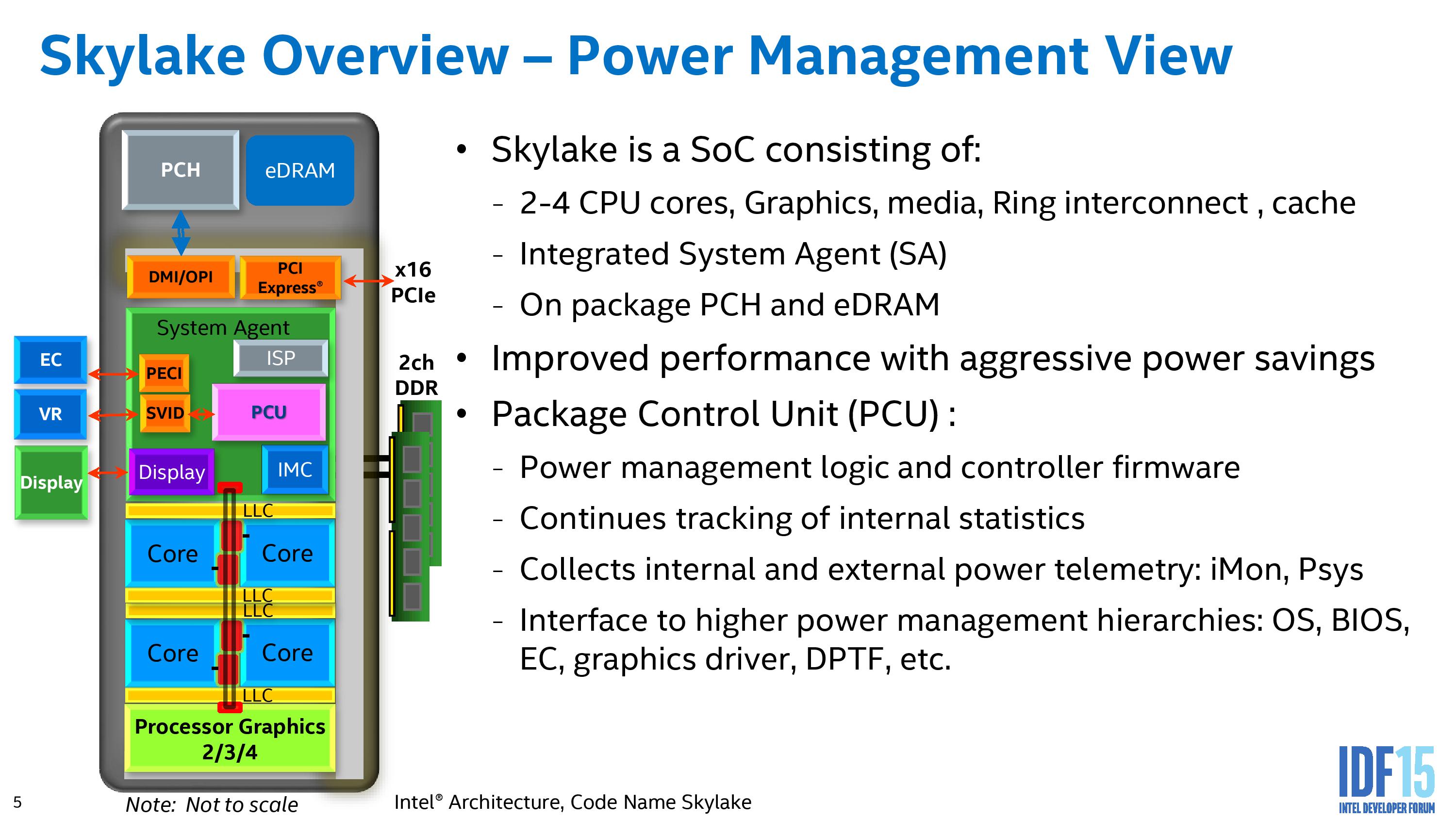
The PCU is essentially a microcontroller (we’ve seen references to a full Intel architecture (IA) core in there) that monitors and computes the power requests and consumption portfolio of the separate silicon areas, providing information that can allow parts of the CPU to be power gated, duty cycled, or adjust in frequency and voltage. We’ve mentioned in our initial Skylake review that going into the CPU itself are four power rails (more with eDRAM). This is an adjustment over Haswell/Broadwell which only had one power rail due to the integrated voltage regulator, which is now moved back on to the motherboard for a combination of reasons related to complexity, efficiency, die area and heat generation.

In all there are at least 12 power gates in a 4+2 design, extending for larger integrated graphics and eDRAM as well. Within this there are several frequency domains – one for core, one for uncore, two for integrated graphics (unslice/slice) and one for eDRAM at a minimum. Being able to react due to power demand and efficiency requirements is a key aspect of Skylake here.
Intel Speed Shift
The new way of managing this comes under the Speed Shift mantra. Intel is promoting this as a faster response vehicle to frequency requests and race to sleep by migrating the control from the operating system back down to the hardware. Based on the presentations, current implementation on P-states can take up to 30 milliseconds to adjust, whereas if they are managed by the processor, it can be reduced to ~1 millisecond. Intel likened this to a car taking a sharp bend, suggesting that a car that can adjust its speed to a greater level of control will take the bend quicker overall. The other factor of Speed Shift is the removal of P-states altogether, which is a different power paradigm to consider.
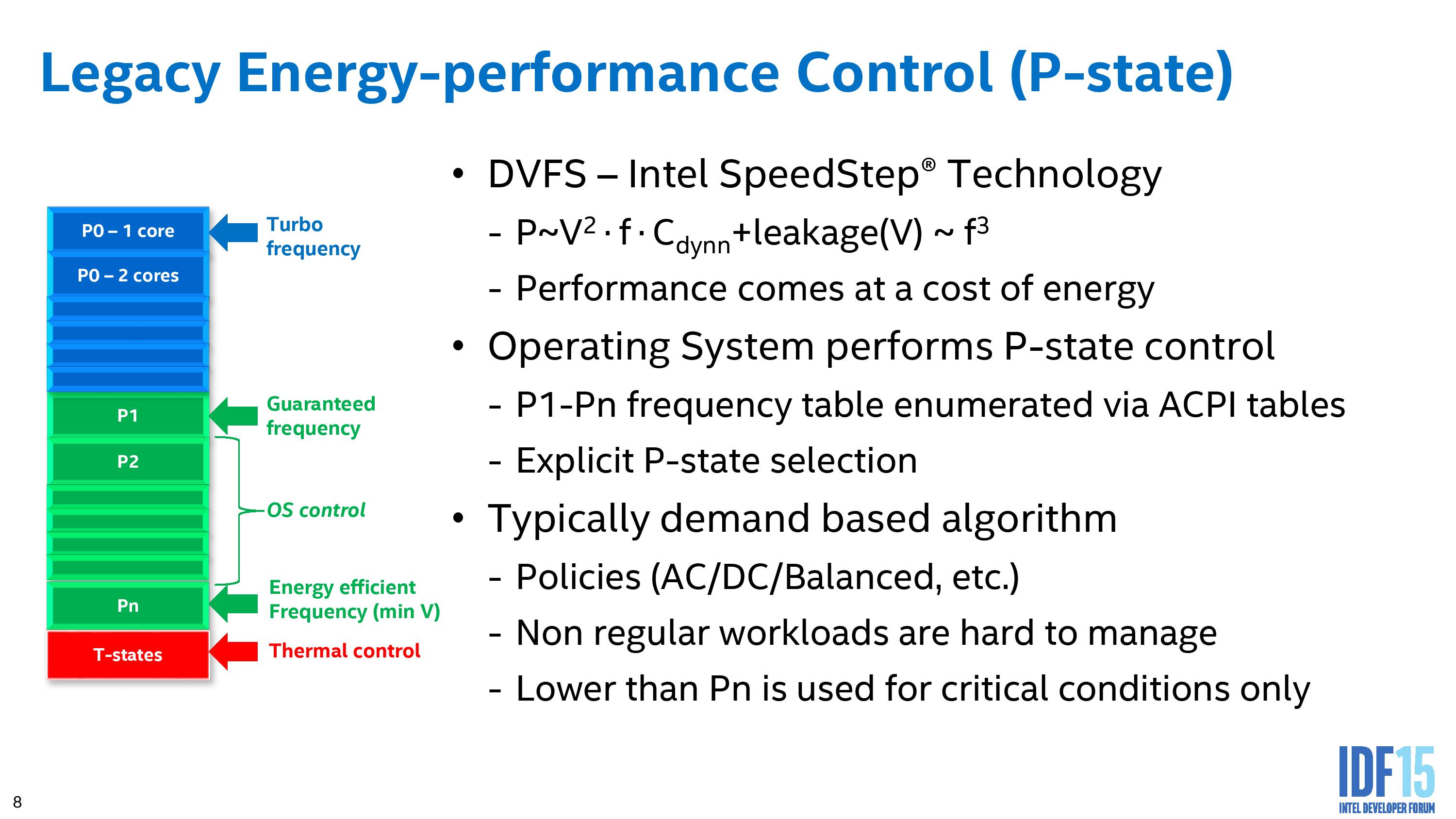
The current implementation provides a P1 frequency (‘on-the-box’) with turbo modes up to P0 and down to Pn where the processor idles at its most efficient implementation. Below this we have thermal management states (T-states) to deal with inappropriate environments to ensure hardware longevity as well as sleep states and low power modes. The P-state table is hardware defined, and the OS flips the switch between them as needed, although the level of granularity is ultimately very course.
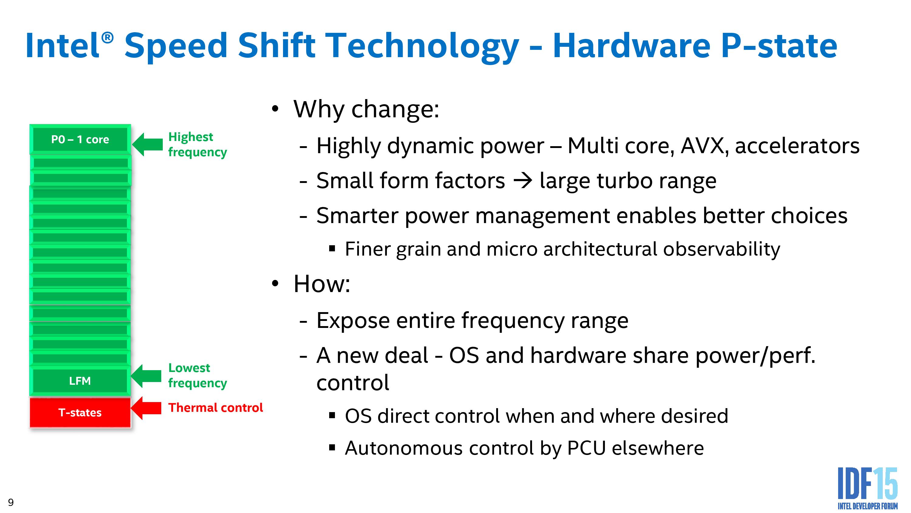
For Speed Shift, the concept moves down to hardware P-states which stretches the range from the lowest frequency on the processor (typically 100 MHz) all the way to the single core turbo frequency (the ‘on-the-box’ turbo) and a finer level of granularity in-between which also allows for quicker changes when necessary to respond to interactions with the system to keep responsiveness high but power consumption low. This makes a lot of sense when we discuss Core M, where the difference between the base and turbo frequency can be as much as 2 GHz in some circumstances.
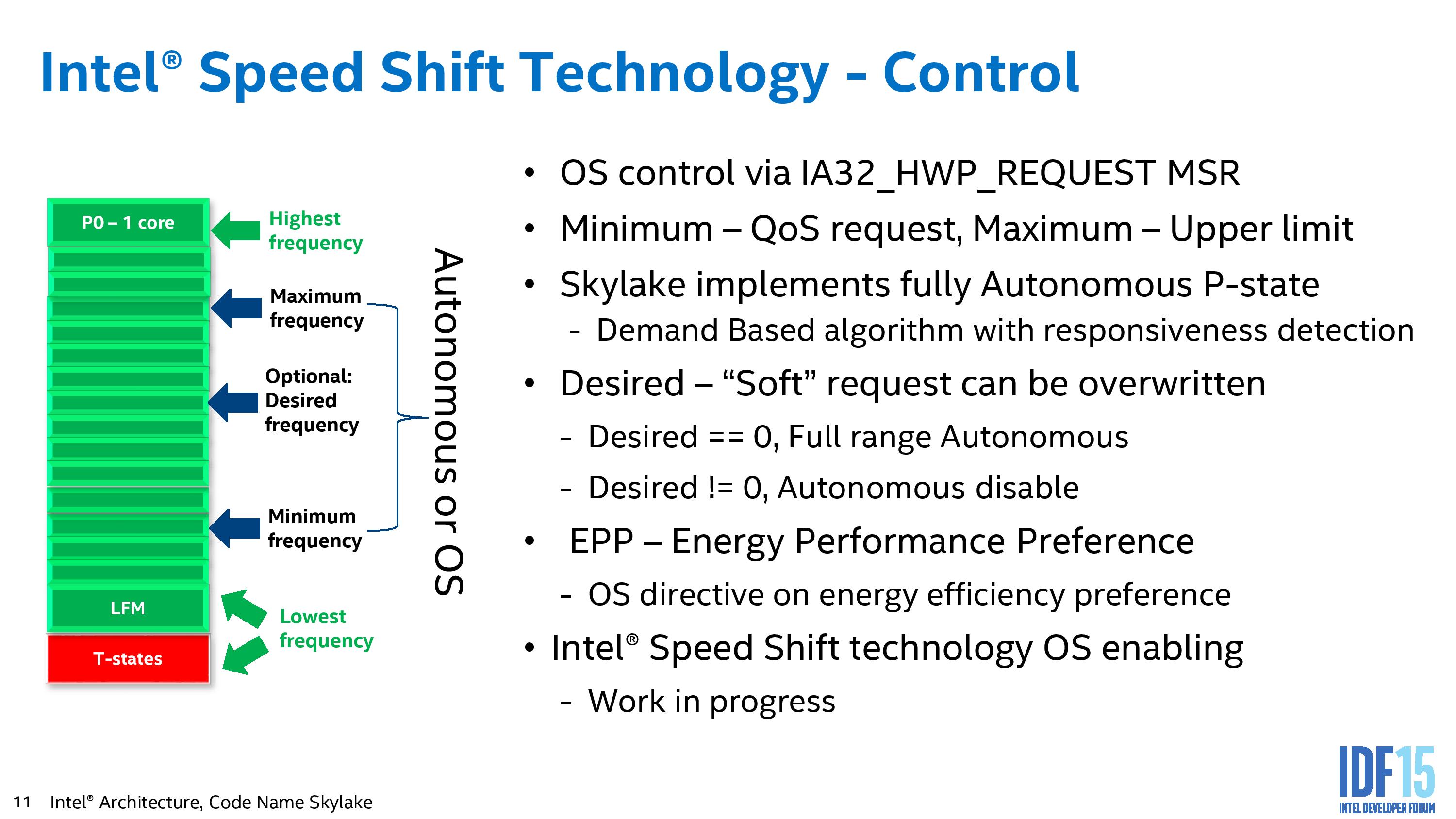
What Speed Shift entails is that ultimately the OS has the highest level of control unless thermal states kick in. The OS can define either the whole of the frequency range (from LFM to P0) or a certain part of that range and hand control back to the processor. This then becomes an ‘autonomous P-state’, allowing the adjustment of frequency to respond on a millisecond timescale. At any time the OS can demand control of the states back from the hardware if specific performance is needed. An overriding factor in all this is that the OS needs to be Speed Shift aware, and currently no operating system is. As you might imagine, Intel is working hard with Microsoft on this to begin with, and it will be part of Windows 10, as there are certain issues in Windows 8.1 and below that do not expose much of the Speed Shift control.
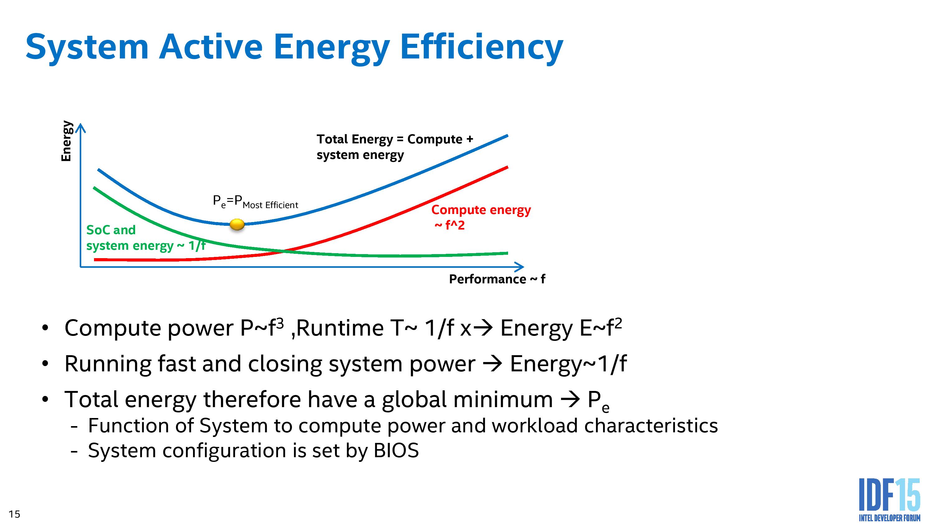
So what the autonomous processor level control will do is come up with the graph above, finding the power state that uses the least total system system power that has been exposed from the operating system. The energy used by the system will have a global minimum for efficiency, and the system will sit here as often as possible. Moving to a lower performance state in this representation actually increases the energy consumption, while moving up the performance curve has the obvious knock on effect on energy use.
It is worth noting at this point that the processor having access to the ‘total’ system power to compute the best position is a new feature of Skylake, called Power of System or Psys.
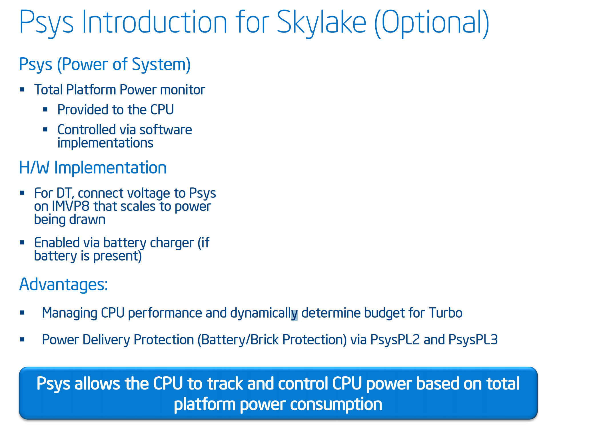
This allows the PCU in the processor to actually profile the performance and power consumption. How the algorithm reacts in this new setting comes within the segment of two Intel derived autonomous algorithms – one for low range and one for high range.
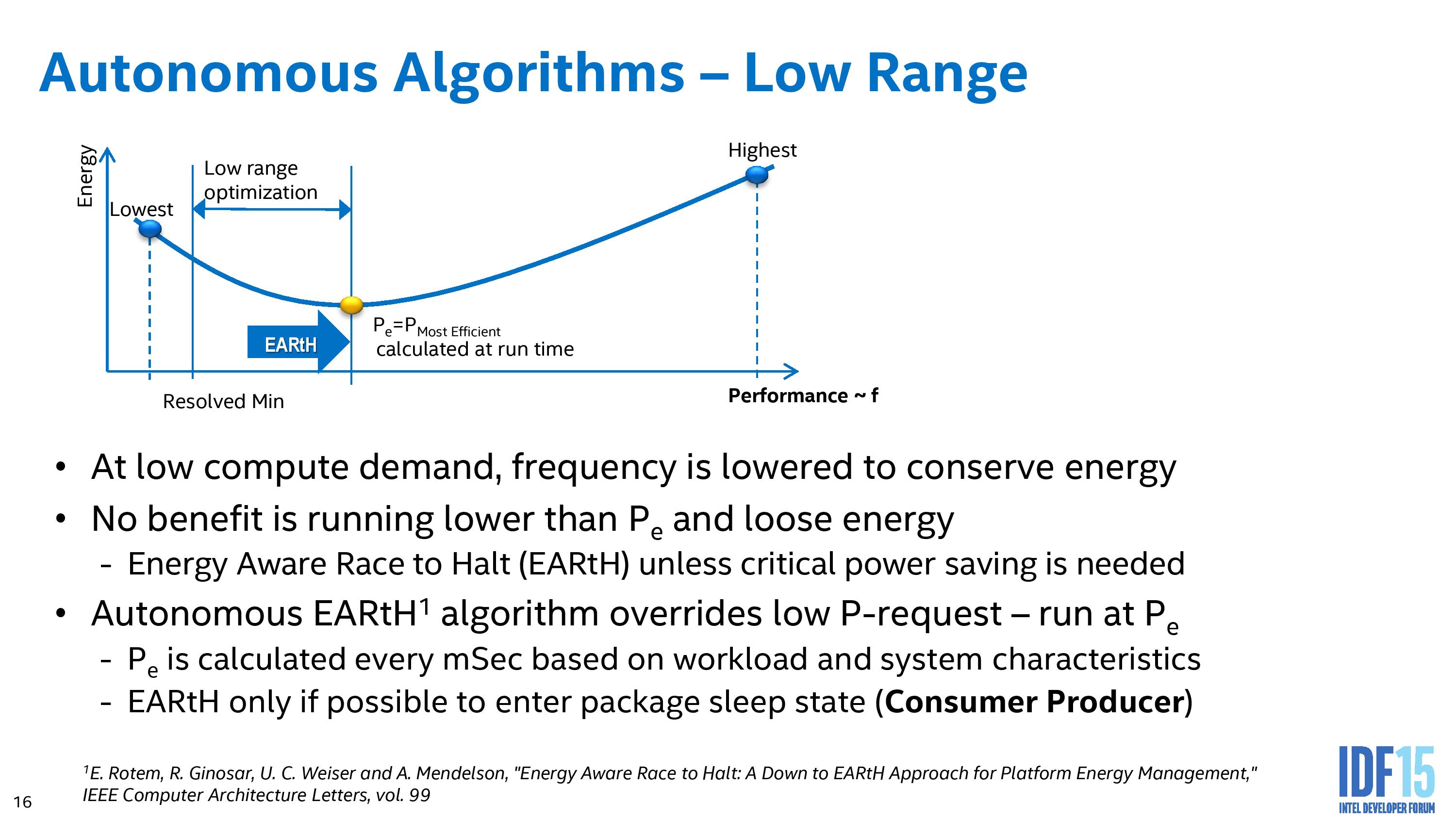

The high range algorithm is of most interest – clearly moving to higher performance affords better response times and quicker time-to-completion, albeit at the expense of energy efficiency. It can be difficult to ascertain whether a user wants something done quickly, or something done efficiency (say, image filters while running on a deadline for a work project compared to image filters casually looking through home photographs). The underlying autonomous algorithm can be preprogrammed (by the OEM or the OS) to respond based on a percentage performance increase for percentage loss in efficiency. This means that some situations might be 1% performance for 2% efficiency, whereas others might go further up the curve to 1%/10% in order to squeeze that extra bit out. Intel’s algorithm also performs an analysis of the workload, whether it is sustained, variable, bursty or can be moved to fixed function hardware, but at any time the OS can jump in and either adjust the algorithm characteristics or take control altogether.
The end goal of Speed Shift is not to increase performance. Running Cinebench at a steady state performance profile will get zero benefit. Intel is aiming specifically at rapidly changing frequency scenarios here, such as office work, moving through PDF documents when images are loading, or conference calls requiring variable load encoding due to data from the camera. Intel stated that web apps, similar to those used in many businesses, are the best test to show benefit, and during IDF Intel warned us (the media) that standard benchmark profiles that speed through user entry significantly faster than a normal user would not see any benefit from Speed Shift.
Update 9/3: We have received word from Intel that Speed Shift will be enabled on all Skylake systems with an up-to-date Windows 10 platform.
Power Control Balancing
At this point, Speed Shift is primarily geared towards the processor cores although there is some level of P-state control in the integrated graphics as well. Under a sustained workload, the power available to the system has to be split to where it is needed, and as we saw in our overclocking of Skylake-K, when you increase the wrong one (CPU) while doing a workload that is dependent on other things (GPU), it can lead to a negative performance difference. By virtue of having access to the total system power, this allows Intel to adjust how it manages that power balance.
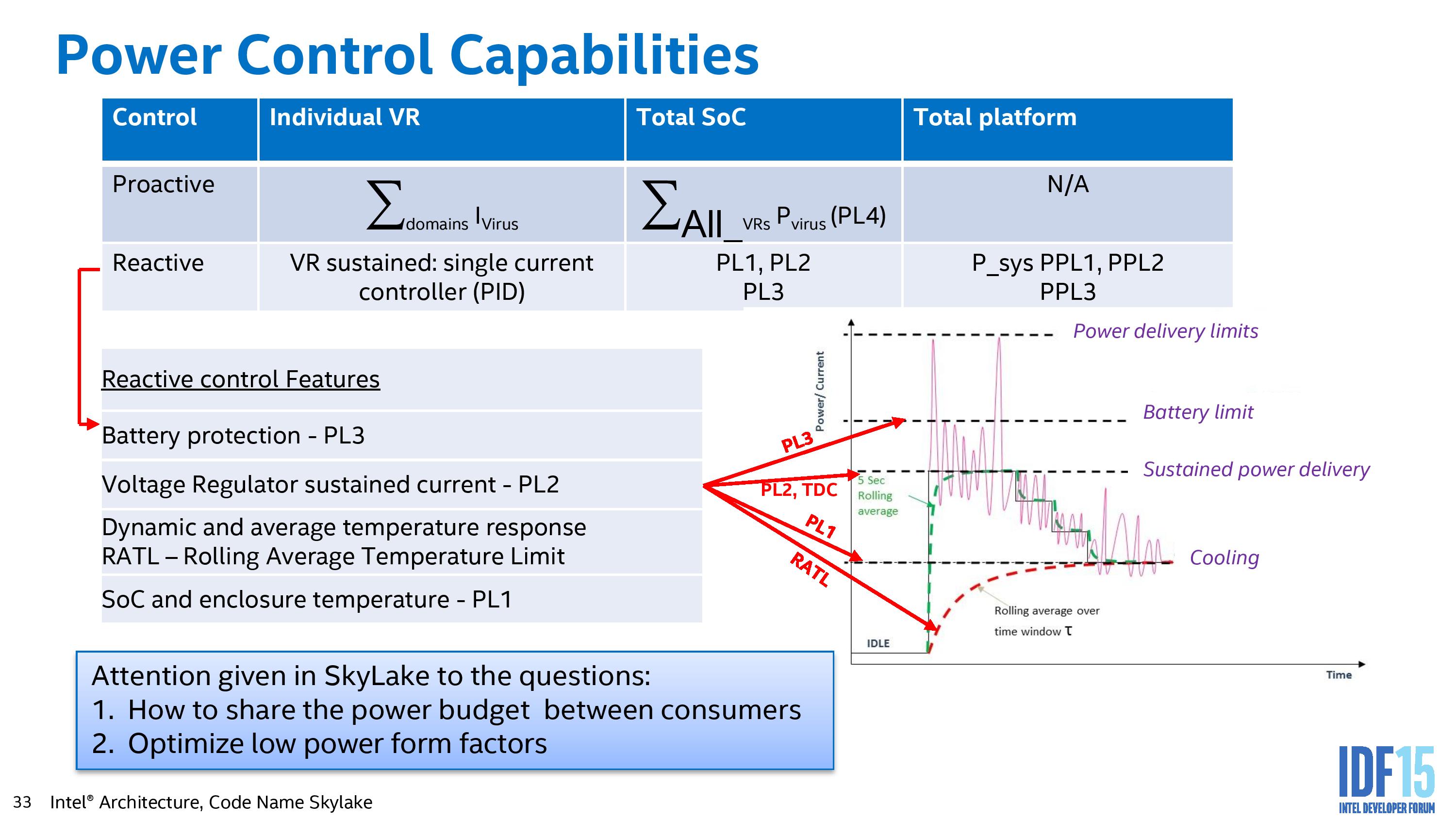
For device OEMs looking at the Skylake-YUH processors, they can define the following characteristics in their system – rolling average temperature limit (RATL), SOC/enclosure temperature (PL1), regulator sustained current (PL2) and battery current protection (PL3). This allows the system to pull up to PL3 from idle very briefly, before being limited to a current drain of PL2 for a short duration then migrating down to PL1 when the system temperature limit is reached as determined by the RATL. This gives the OEM a good fine control on the limits of the system, but distribution of this power comes to the workload aware balancer.

The controller monitors the workload in question based on data transfer and compute, and then can split the power states as required between the cores, graphics and system in order to keep the sum power within the PL1 limit. As shown in the diagram above, the balancer can only give to one when it takes from another, and where possible it will consider which elements of the system might provide better efficiency while keeping performance as expected.
Duty Cycling
Throughout all of the power optimizations mentioned so far – and indeed many of the power optimizations at the heart of the Core architecture over many generations – has been the concept of race to idle or race to sleep. The idea is simple enough: get the job done as soon as you can and then get the CPU back to an idle state. This is an effective strategy because processors operate on a voltage/frequency curve, resulting in higher power consumption at higher frequencies, and conversely power consumption quickly drops at lower frequencies.
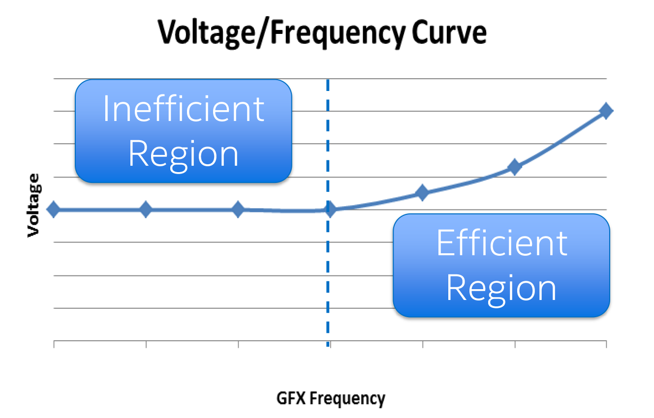
However as Intel seeks to further optimize their power consumption, they have been running headlong into the laws of physics. The voltage/frequency curve is just that, a curve, meaning that it flattens out towards the bottom. As it turns out it flattens out more rapidly than you’d think due to the existence of a threshold voltage for transistors, which is the minimum voltage required for a transistor to operate. As a result of this effect, idling at even lower frequencies sees rapidly diminishing returns once you drop below the threshold voltage, and at this point reducing frequencies is no longer an effective way to reduce power consumption.
In Broadwell, Intel introduced the idea of Duty Cycle Control (DCC) to solve the idle power savings problem for the processor’s iGPU. A solution that is both a bit brute force and a bit genius, with DCC Intel outright shut off the iGPU for a period of time, rapidly cycling between the on and off states, the process of duty cycling. With DCC Intel was able to save power in a very straightforward manner, bypassing the idle power problem entirely and just not running the iGPU when it wasn’t needed. While there is a small amount of overhead to waking the iGPU up and putting it back to sleep, the relative power savings from DCC were close to the overall amount of time the iGPU was turned off.
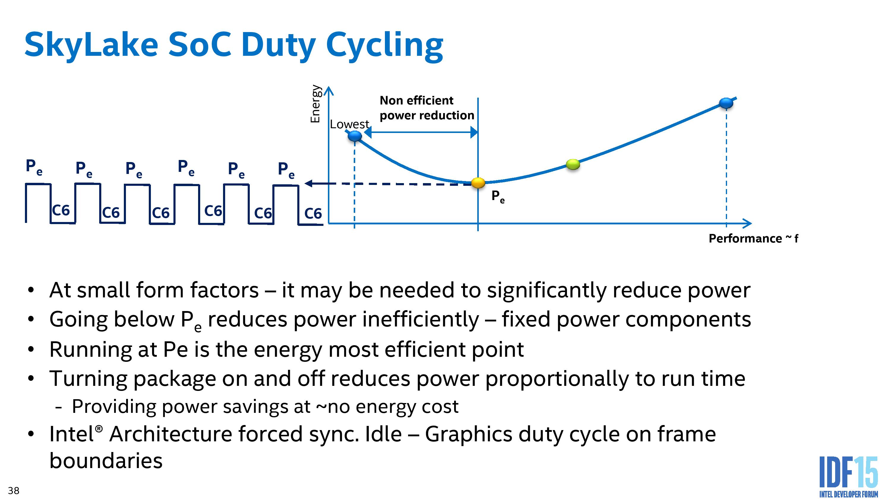
Catching up to Skylake then, Intel has taken the duty cycle concept to the next stage and implemented DCC on the CPU cores as well. Similar to Broadwell’s iGPU implementation, this involves rapidly turning the CPU cores off and on to achieve further power savings beyond what idling alone can offer. In the case of Skylake this process can occur as often as every 800 microseconds, with Intel picking a point that balances the cost of transitioning with the need to avoid having the CPU stay off for longer than the OS can handle. In the slide above, the duty cycle rate is set at 50%, with equal time between Pe and C6, although this can be adjusted as needed.
Of all of the power saving features introduced in Skylake, duty cycling the CPU cores is likely to be among the most potent of these features. Duty cycling allows Intel to reap many of the power benefits of C6 sleeping without the cost of fully going to sleep from an OS perspective, and it allows Intel to cover edge cases where a workload is present that requires the CPU cores to remain awake without doing much in the way of actual work. Put another way, duty cycling on Skylake allows Intel to fully maximize the amount of time the CPU cores and the iGPU are kept in low-power sleep states.
Back to the L2 Cache
In order to make the power section more complete, we want to cycle back to our L2 cache power saving scenario. Several pages ago in the CPU architecture page, we mentioned that there are changes to the L2 cache that have a knock on effect on power. What Intel has done in Skylake is reduce the L2 cache associativity (the way it tracks cache data) from an 8-way design to a 4-way design. This has two effects – power savings but performance penalties. Since at least Sandy Bridge (and even before), Intel has always stayed with an 8-way L2 design per core on its main performance architectures, so moving to 4-way was a little surprising. Speaking to Intel, the power savings are significant enough to do this, and they have put measures in place such that the L2 cache miss latency and bandwidth are both significantly improved in order to hide the performance difference this change it might create. We are also told that this change allows their corporate and enterprise platforms an extra element of adjustment, and we should keep an eye on these when the E5 processors are released (which by our estimates is at least 2017?).
Other Enhancements
Aside from Speed Shift, the L2 cache, and our previous notes regarding fixed function hardware in the graphics, Intel has a few other power considerations.
With power in mind, Intel also pressed home during IDF about a general efficiency improvement across the board, extending to the ring in the core, a digital PLL, serial power IO and advanced power management. As mentioned before, Intel has moved the integrated voltage regulator (FIVR) that we saw in Haswell and Broadwell back out of the processor, leaving it in the domain of the motherboard. There was no clear cut answer to this, but it is known that FIVRs are not always very efficient at low loads and can cause high die temperatures when under stress. By moving it to the motherboard, it becomes an external issue. There is the potential for Intel to use linear regulators at low power, although as we understand these do not scale in ways that Intel can find them to be beneficial to the design process. We are getting big hints that we will most likely see the FIVR move back on to the design, although it is unclear if this will result in a specific design focus or if it will happen across the board.


173 Comments
View All Comments
just4U - Wednesday, September 2, 2015 - link
I have to agree with Jumangi,If your gaming plans revolve around a integrated GPU your still better served to go the AMD route.. While the CPU is not as fast it's no slouch either.. and gaming performance is going to be acceptable in comparison on most titles.
sundragon - Monday, September 7, 2015 - link
Um, first hand experience: Macbook Pro 2015, (Iris 6200): Skyrim, ESO, Civilization 5, Homeworld, all run at 1440x - I love all these people talk about intel integrated graphics sucking, meanwhile I'm getting crushed in Civ5 and kicking ass in Homeworld and ESO.I'm not lugging an integrated laptop around to play games, I have a laptop and I like to have ONE LAPTOP, and guess what, everything I've thrown on here has played. My MBA 2012 HD4000 struggled with Skyrim and Civ 5 but I still played. Please stop talking theoretical and talk about your actual rig... /end rant
BurntMyBacon - Thursday, September 3, 2015 - link
@retrospooty: Core2 era was more a return to parity. One of the most even matchups I can remember was the ironically similarly numbered Phenom II 955 and the Core 2 Quad 9550. Nahalem is what really did the damage. Here's hoping Zen can put AMD back in the ballpark.I do think AMD has a pretty significant GPU advantage in the area of gaming over Intel. However, as you've stated, the power/thermal constraints do not allow them to fully exploit this advantage. A CPU intense game, even if not CPU limited, will chew up much of the GPU's available thermal envelop, effectively eliminating any advantage AMD had. Granted, there are cases where the thermal solutions in play provide the necessary thermal headroom, but these are mostly found in laptops that are already using discrete chips.
MrBungle123 - Thursday, September 3, 2015 - link
The Phenom II didn't come out until after Intel had retired the Core 2 line. Everyone wants AMD to be competitive but the fact is they are miles behind Intel.MapRef41N93W - Friday, September 4, 2015 - link
Guess you didn't read the review of Broadwell Iris Pro on this very site. AMD's GPU loses by as much as 20-30% in most games vs Broadwell Iris Pro. Skylake Iris Pro will be offering up to 50% more performance.V900 - Wednesday, September 2, 2015 - link
4: Not everybody who are interested in a gaming machine can afford a Core i7 and several 1000$ graphic cards in a SLI configuration. A lot of gamers have a budget between 500$-1000$, and if you can get/get close to XB1 performance with just an Intel IGP, it would be perfect for that kind of budget.Also: Why would you think a 13' laptop with Iris Pro and 72 execution units would "fail miserably" in comparison with an XB1/PS4?!?
That's ridiculous. Any advantage the console would have is tiny.
Just get two wireless controllers and hook up the laptop to your HDTV with a HDMI cable, and the experience would be close to identical....
MrSpadge - Wednesday, September 2, 2015 - link
"Also: Why would you think a 13' laptop with Iris Pro and 72 execution units would "fail miserably" in comparison with an XB1/PS4?!?"Because he specifically mentioned this in conjunction with "user experience". The PC gives you freedom but certainly not the ease of use of a console. Which is mainly why these things exist at all.
Jumangi - Wednesday, September 2, 2015 - link
Lolz if you think an Intel only machine with any sort of Integrated graphics(even the best Iris Pro) will give you anything close to an Xbox One game your seriously naive and ignorant. Stop looking at theoretical Gflops numbers to make comparisons.IanHagen - Wednesday, September 2, 2015 - link
Well, a few posts back up you're stating that AMD's A10 APU have "far better graphics" when it failed to beat last generation Iris 5200 GPU and now there you are, talking about naiveness and ignorance.Jumangi - Wednesday, September 2, 2015 - link
Compare actual gaming on the two mr naive one. also compare the huge cost differences of these chips. An Iris Pro laptop will be far far more expensive.