HBM4 in Development, Organizers Eyeing Even Wider 2048-Bit Interface
by Anton Shilov on October 12, 2023 10:00 AM EST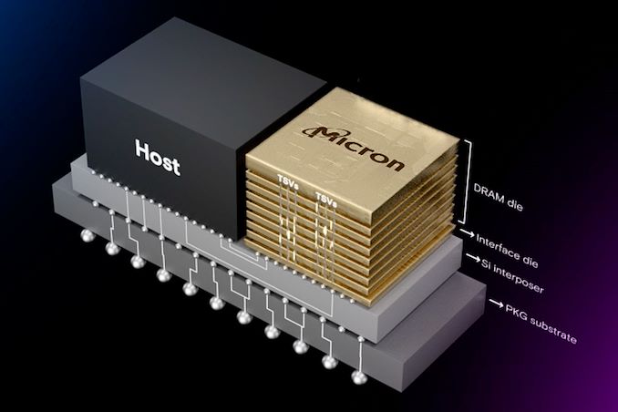
High-bandwidth memory has been around for about a decade, and throughout its its continued development it has steadily increased in speed, starting at a data transfer rate from 1 GT/s (the original HBM) and reaching upwards of 9 GT/s with the forthcoming HBM3E. This has made for an impressive jump in bandwidth in less than 10 years, making HBM an important cornerstone for whole new classes of HPC accelerators that have since hit the market. But it's also a pace that's getting harder to sustain as memory transfer rates increase, especially as the underlying physics of DRAM cells have not changed. As a result, for HBM4 the major memory manufacturers behind the spec are planning on making a more substantial change to the high-bandwidth memory technology, starting with an even wider 2048-bit memory interface.
Designed as a wide-but-slow memory technology that utilizes an ultra-wide interface running at a relatively modest clockspeed, HBM's current 1024-bit memory interface has been a defining characteristic of the technology. Meanwhile its modest clockspeeds have become increasingly less modest in order to keep improving memory bandwidth. This has worked thus far, but as clockspeeds increase, the highly parallel memory is risking running into the same signal integrity and energy efficiency issues that challenge GDDR and other highly serial memory technologies.
Consequently, for the next generation of the technology, organizers are looking at going wider once more, expanding the width of the HBM memory interface even further to 2048-bits. And, equally as important for multiple technical reasons, they intend to do this without increasing the footprint of HBM memory stacks, essentially doubling the interconnection density for the next-generation HBM memory. The net result would be a memory technology with an even wider memory bus than HBM today, giving memory and device vendors room to further improve bandwidth without further increasing clock speeds.
As planned, this would make HBM4 a major technical leap forward on multiple levels. On the DRAM stacking side of matters, a 2048-bit memory interface is going to require a significant increase in the number of through-silicon vias routed through a memory stack. Meanwhile the external chip interface will require shrinking the bump pitch to well below 55 um, all the while increasing the total number of micro bumps significantly from the current count of (around) 3982 bumps for HBM3.
Adding some additional complexity to the technology, memory makers have indicated that they are also going to stack up to 16 memory dies in one module; so-called 16-Hi stacking. (HBM3 technically supports 16-Hi stacks as well, but so far no manufacturer is actually using it) This will allow memory vendors to significantly increase the capacity of their HBM stacks, but it brings new complexity in wiring up an even larger number of DRAM dies without defects, and then keeping the resulting HBM stack suitably and consistently short.
All of this, in turn will require even closer collaboration between chip makers, memory makers, and chip packaging firms in order to make everything come together smoothly.
Speaking at TSMC's OIP 2023 conference in Amsterdam, Dan Kochpatcharin, TSMC's Head of Design Infrastructure Management had this to say: "Because instead of doubling the speed, they doubled the [interface] pins [with HBM4]. That is why we are pushing to make sure that we work with all three partners to qualify their HBM4 [with our advanced packaging methods] and also make sure that either RDL or interposer or whatever in between can support the layout and the speed [of HBM4]. So, [we work with] Samsung, SK Hynix, and Micron."
Since system-in-package (SiP) designs are getting larger, and the number of HBM stacks supported by advanced chip packages is increasing (e.g. 6x reticle size interposers and chips with 12 HBM stacks on-package), chip packages are getting more complex. To ensure that everything continues to work together, TSMC is pushing chip and memory designers to embrace Design Technology Co-Optimization (DTCO). This being a big part of the reason why the world's largest foundry recently organized 3DFabric Memory Alliance, a program designed to enable close collaboration between DRAM makers and TSMC in a bid to enable next-generation solutions that will pack huge amounts of logic transistors and advanced memory.
Among other things, TSMC's 3DFabric Memory Alliance is currently working on ensuring that HBM3E/HBM3 Gen2 memory works with CoWoS packaging, 12-Hi HBM3/HBM3E packages are compatible with advanced packages, UCIe for HBM PHY, and buffer-less HBM (a technology spearheaded by Samsung).
Overall, TSMC's comments last week give us our best look yet at the next generation of high-bandwidth memory. Still, additional technical details about HBM4 remain rather scarce for the moment. Micron said earlier this year that 'HBMNext' memory set to arrive around 2026 will offer capacities between 36 GB and 64 GB per stack and peak bandwidth of 2 TB/s per stack or higher. All of which indicates that memory makers won't be backing off on memory interface clockspeeds for HBM4, even with the move to a wider memory bus.


11 Comments
View All Comments
Threska - Thursday, October 12, 2023 - link
One wonders if optical links would be better in speeding up the links between memory and CPU.Reflex - Thursday, October 12, 2023 - link
Unlikely for performance, electricity over copper also moves at very close to the speed of light. It could for power consumption, but that depends on how far you want the memory from the CPU. If it's close then you probably don't gain anything due to conversion losses (the signals still need to be converted back to electricity at either end). If further away, then it may provide a benefit despite conversion.shing3232 - Friday, October 13, 2023 - link
You still need to convert it into light signal through and there is delay for that.saratoga4 - Friday, October 13, 2023 - link
Optical links are mostly used for longer range. Once you're within centimeters they don't make a lot of sense.Kevin G - Thursday, October 12, 2023 - link
I'd be nice to see some more exotic memory techniques appear in HBM. For example, separated read/write buses to remove all turn around time latencies. Similarly, create a dedicated command bus. These three buses (read, write, command) can be defined at different widths and clocks in the spec as well as permit independent clocks on the each bus for power savings. These changes would increase the complexity of the memory controller but that is the price of exotic memory technologies like HBM in the first place.meacupla - Thursday, October 12, 2023 - link
2048bit bus is crazy.I would be happy if we could have 256bit bus on a low end GPU.
schujj07 - Thursday, October 12, 2023 - link
That is 2048 bit per stack. A GPU with 4 stacks on HBM4 would have an 8192 bit bus.Oxford Guy - Friday, October 13, 2023 - link
Bit of trivia: My recollection is that AMD’s Fiji had 2048-bit HBM1 bus. That went to 1024 bits with Vega (HBM2).Kevin G - Friday, October 13, 2023 - link
Fiji was 4096 bit wide with four stacks of HBM1. Vega 64 had two stacks of HBM2 for a 2048 bit width. Radeon VII went to four stacks again while the rarely seen mobile Vega had a single stack at 1024 bits wide. This mobile Vega part is what was used inside Intel's Skull Canyon NUC.The largest number of HBM stacks on a product I've seen so far is eight (8192 bit width) for the MI300 series but that is where each chiplet has its own HBM stack. There are a few large monolithic dies with six stacks (6144 bit width). Technically possible to go to even greater number stacks but the extra interposers and packaging headaches are not yet worth it. With products like nVidia's H100 being able to have a single layer of a stack disabled, the yield factor of packaging may not be that significant of an issue.
Oxford Guy - Friday, October 13, 2023 - link
'Fiji was 4096 bit wide with four stacks of HBM1. Vega 64 had two stacks of HBM2 for a 2048 bit width.'Don't get old.