Apple Announces A8 SoC
by Ryan Smith on September 9, 2014 1:45 PM EST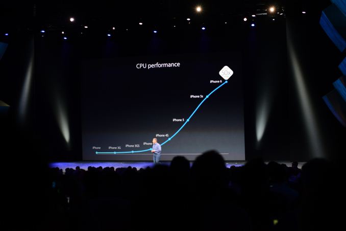
As expected from this year’s iPhone keynote, Apple has announced a new member of their internally developed family of ARM SoCs.
The latest SoC, dubbed A8, is Apple’s first SoC built on the 20nm process, and among the first SoCs overall to be built on this process. Apple notes that it has 2 billion transistors and is 13% smaller than the A7, which would give it upwards of twice as many transistors as the A7 and would put the die size at about 89mm2.
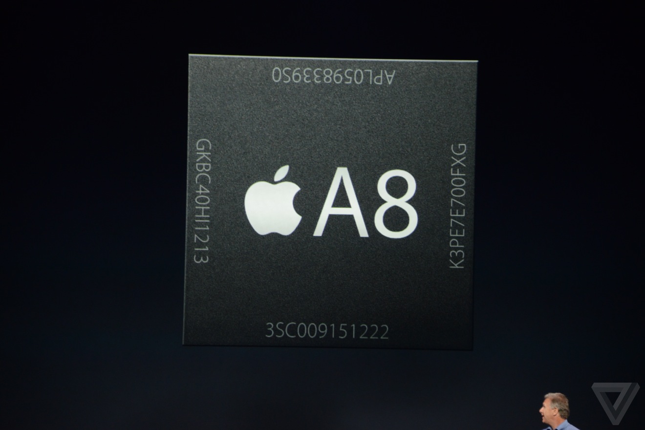
Image courtesy The Verge
From a performance perspective Apple is promising 25% faster CPU performance than A7. As is usually the case with Apple, they aren’t talking about the underlying CPU core – though this is a problem we’re working to rectify – so it remains to be seen how much of this is due to CPU architectural upgrades and how much is from clockspeed improvements afforded by the 20nm process. Apple just introduced their 64bit Cyclone core last year, so it stands to reason that just a year later and with the transition to 64bit already completed, A8 packs a CPU that is similar to Cyclone.
| Apple SoC Evolution | |||||
| CPU Perf | GPU Perf | Die Size | Transistors | Process | |
| A5 | ~13x | ~20x | 122m2 | <1B | 45nm |
| A6 | ~26x | ~34x | 97mm2 | <1B | 32nm |
| A7 | 40x | 56x | 102mm2 | >1B | 28nm |
| A8 | 50x | 84x | 89mm2 | ~2B | 20nm |
Meanwhile Apple is being even less specific about the GPU, but from their published baseline performance comparisons against the iPhone 1, the A8 is said to be 84x faster on graphics. This compares to a published figure of 56x for the A7, which implies that the A8’s GPU is 1.5x faster than the A7’s. Given Apple’s conservative stance on clockspeeds for power purposes and the die space gains from the 20nm process, it seems likely that Apple has upgraded from a 4 core PowerVR GPU to a 6 core PowerVR GPU, likely the flagship GX6650, which would account for the 50% performance gain right there.
Finally, Apple notes that the A8 is designed to be 50% more energy efficient than the A7. Some of these efficiency gains would come from gains due the 20nm process, however this large of a gain would indicate that Apple has done additional work at the architectural level to improve efficiency, as smaller manufacturing nodes alone do not see these kinds of gains.
Update: We have posted our initial A8 analysis here


66 Comments
View All Comments
ancientarcher - Tuesday, September 9, 2014 - link
So, A8 has 2bn transistors vs 1bn for A7. But CPU is only 25% faster, maybe due to a higher clockspeed (which means same number of xtors for the CPU) and GPU is only 50% faster. If GPU was 50% of the area of A7, then that means another 250mn xtors for the A8 GPU vs A7.So, question is - what is the use of the other 750mn xtors?? seems a large number of xtors to waste...
And yes, the transistor density seems to higher than the 14nm Core-M from Intel ;-P
Achtung_BG - Tuesday, September 9, 2014 - link
Apple A7all is 102mm2, 2 core CPU is 17mm2 and GPU is 22mm2.tipoo - Tuesday, September 9, 2014 - link
Larger L3/GPU cache?Kevin G - Tuesday, September 9, 2014 - link
That would be my bet as well.They also mentioned a new image sensor unit, so that likely accounts for a bit too.
tipoo - Tuesday, September 9, 2014 - link
The above post also assumes transistors scale with performance perfectly, it may take a lot more transistors just for that 50% GPU increase.DERSS - Saturday, September 13, 2014 - link
It could be RAM; now it is 2 GB versus 1 GB in A7.Remember that A8 is multi-layer system on chip, so 2 billion is total count of transistors in it.
anderct - Monday, September 15, 2014 - link
still 1GB of RAM and the SOC does not dictate actual program RAM use.witeken - Tuesday, September 9, 2014 - link
It is unlikely that 20nm is more dense than Intel's 14nm process: http://image.ofweek.com/uploadfile/newsimg/b/2014/...One thing that you have to keep in mind is that Intel always publishes their schematic transistor count. The real transistor count is likely quite a bit higher.
The main reason why this claim from Apple doesn't seem right is because if they doubled the amount of transistors and reduced the die area by 25%, this is a lot more than the 1.9X increase in density that was claimed.
Gondalf - Tuesday, September 9, 2014 - link
The reason is simple, A7 had >1B transistors, this means likely 1.5B or so but Apple never told us :Pmkozakewich - Tuesday, September 9, 2014 - link
They could also have reduced non-transistor die area.