Samsung SSD 850 Pro (128GB, 256GB & 1TB) Review: Enter the 3D Era
by Kristian Vättö on July 1, 2014 10:00 AM ESTRandom Read/Write Speed
The four corners of SSD performance are as follows: random read, random write, sequential read and sequential write speed. Random accesses are generally small in size, while sequential accesses tend to be larger and thus we have the four Iometer tests we use in all of our reviews.
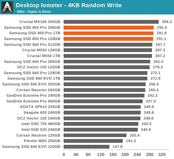
Our first test writes 4KB in a completely random pattern over an 8GB space of the drive to simulate the sort of random access that you'd see on an OS drive (even this is more stressful than a normal desktop user would see). We perform three concurrent IOs and run the test for 3 minutes. The results reported are in average MB/s over the entire time.
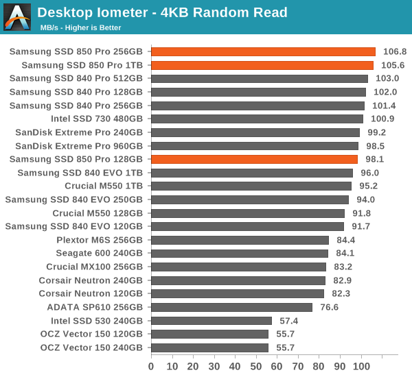
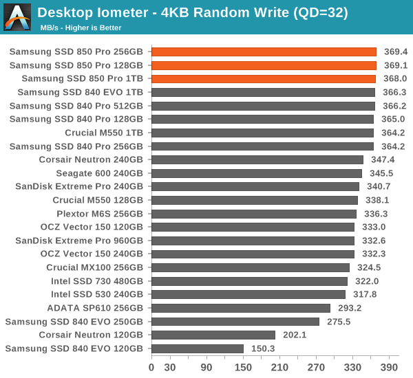
Random performance is also brilliant and the 850 Pro tops almost all of our benchmarks. It is no wonder why it is so fast in the Storage Benches.
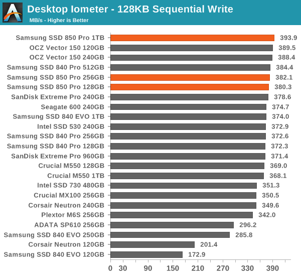
Sequential Read/Write Speed
To measure sequential performance we run a 1 minute long 128KB sequential test over the entire span of the drive at a queue depth of 1. The results reported are in average MB/s over the entire test length.
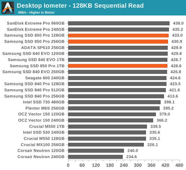
The same goes for sequential speeds. Of course, the differences are not substantial but nevertheless the 850 Pro is fast.
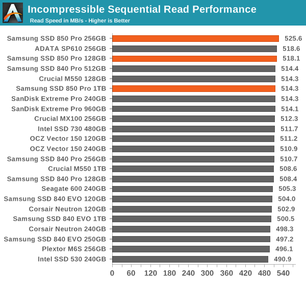
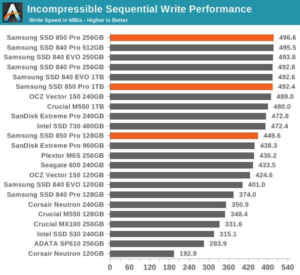
AS-SSD Incompressible Sequential Read/Write Performance
The AS-SSD sequential benchmark uses incompressible data for all of its transfers. The result is a pretty big reduction in sequential write speed on SandForce based controllers, but it doesn't impact most of the other controller much if at all.


160 Comments
View All Comments
Squuiid - Saturday, March 14, 2015 - link
Plus, the MX100 reliability is horrible. Just google MX100 BSOD, disappearing drive.I have 2x MX100 512GB SSDs and I recommend you don't buy one, no matter how cheap they are.
nightauthor - Tuesday, July 1, 2014 - link
For business purposes, I would rather pay twice as much and get a 10 year warranty vs the 3 year supplied by Crucial. Though, for my daily, I would probably go with the Crucial.TheWrongChristian - Wednesday, July 2, 2014 - link
No current SATA drives push low queue depth random IOs to the point of saturating SATA II, let alone SATA III.At high queue depths, perhaps. But then, that is not a typical workload for most users, desktop or server.
Plus, it's a new drive, prices will come down.
jwcalla - Monday, June 30, 2014 - link
Unless they're doing 5% OP the capacities are kinda... off.melgross - Monday, June 30, 2014 - link
I think there's a slight misunderstanding of manufacturing cost. While the die size may be the same, or even smaller than a competing technology, the 32 level chip does cost more to make per area. There are more masks, more layers, more etching and washing cycles, and more chance of defects.Right now, I do see why the cost is higher. I can on,y assume that as this technology progresses, that cost will drop per area. But it will always remain higher than an SLC, MLC or TLC chip.
So there is a balance here.
Kristian Vättö - Tuesday, July 1, 2014 - link
You are correct. I did mention yield and equipment cost in the final paragraph but I figured I won't go into detail about masks and etching since those would have required an in-depth explanation of how NAND is manufactured :)R0H1T - Tuesday, July 1, 2014 - link
It would be great if Anand or you do a writeup on 3d NAND & deal with the specific pros & cons of it as compared to traditional 2d NAND & if possible include something related to manufacturing processes of these & how they're different OR more/less expensive, certainly as in case of V-NAND?MrSpadge - Tuesday, July 1, 2014 - link
You wouldn't need too much detail - just saying that the number of process steps increases by probably around an order of magnitude should make this pretty clear.frenchy_2001 - Tuesday, July 1, 2014 - link
It is probably more than that, as Samsung is currently manufacturing 32 layers of cells. Each layer requires multiple operations (deposit, etching, washing...). Their biggest advantage comes from regressing to 40nm: at that technology, each operation is *MUCH* cheaper than the equivalent one at 1X pitch (15~19nm).So, total cost is an unknown, but should be very competitive, after recovering the initial R&D investment.
Spatty - Tuesday, July 1, 2014 - link
And not to mention 3D NAND is still basically bleeding edge. It's still in the stages of where a new DDR generation arrives, much higher costs then current gen.